NVIDIA 680i: The Best Core 2 Chipset?
by Gary Key & Wesley Fink on November 8, 2006 4:45 AM EST- Posted in
- CPUs
nForce 680i Overclocking
The defining area for the 680i chipset has to be overclocking. The 500 family chipsets for Intel performed fine in many areas, but they were one of the worst chipsets available for Intel in overclocking, topping out somewhere below 350 MHz on the bus speeds. This area kept many Enthusiasts from embracing the NVIDIA SLI solution for their Core 2 processors. It appeared NVIDIA had designed the 500 chipset family for spectacular overclocking on the 200 MHz HTT AMD AM2 chipset. The problem, of course, is that Core 2 processors were released at 1067 FSB (266 base bus speed), and the 500 family chipsets did not have anywhere close to the headroom of the competing Intel chipsets.
All of that has changed, NVIDIA tells us, with a 680i that can do 1333 FSB and more and DDR2 memory speeds of 1200 and beyond. To test NVIDIA's claims we tested the EVGA 680i SLI using the following setup:
The overclock results are not a mistake. We managed to reach right at 4.0GHz with an X6800 at 1.575V. This represented the standard 11x ratio at a 1452 FSB. Even more spectacular was the reduced multiplier overclocking, where we reached a 2100 FSB (525 base) at a 7X multiplier AT DEFAULT VOLTAGE.
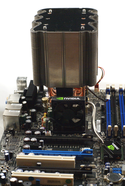
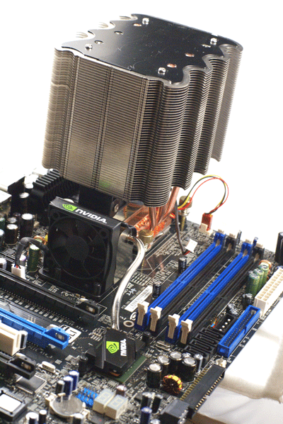
These results were with air cooling using a Tuniq 120 air cooler, which sandwiches a 120mm fan in a finned heatpipe core as pictured above.
One of our X6800 processors reached 2100 FSB, confirming NVIDIA's claims of overclocking an X6800 in their labs to 2070 FSB. Not only did we reach 2100 FSB (525) at a 7X multiplier (3.675GHz), we managed to reach that speed at default voltage. The system has run at those settings for several days without incident and has handled every test and benchmark we have thrown at the system. However, it should also be pointed out that a second X6800 CPU would not overclock 1 MHz higher than 1900 FSB (450) on this same motherboard, even though that X6800 reached a similar 4GHz maximum overclock and similar "default voltage" overclocks.
We have yet to find anything obvious that would explain these differences in maximum FSB in the X6800 chips we tested. Revision and Stepping explained nothing, and we also had four retail E6600 we tested that would not reach above 1800 FSB. We are looking into these findings further and hope to find some explanations to share with you that will explain these maximum FSB differences among 4MB Cache Core 2 chips.
Interestingly, all of the 2MB cache Core 2 processors we tested reached at least 2000 FSB, with the two tested E6300 reaching 2100 FSB (522x7 and 6x525). We were prepared to call the amount of cache the defining difference in FSB performance until the late X6800 reached 2100 in our labs and NVIDIA confirmed their own 2070 results with an X6800 Extreme. We are much more confident that 2MB Cache chips can top 2000 FSB and we are very anxious to find something that will help you identify 4MB cache chips that will reach the "magic" 2000, 2070, and 2100 FSB overclocks.
Overall overclocking performance with the 680i was spectacular, and the results should excite any of you who want to do some serious overclocking with a Core 2 processor. At the very least the nForce 600i chipset family gives shoppers new choices in motherboards that will make the most of their Core 2 processor.
The defining area for the 680i chipset has to be overclocking. The 500 family chipsets for Intel performed fine in many areas, but they were one of the worst chipsets available for Intel in overclocking, topping out somewhere below 350 MHz on the bus speeds. This area kept many Enthusiasts from embracing the NVIDIA SLI solution for their Core 2 processors. It appeared NVIDIA had designed the 500 chipset family for spectacular overclocking on the 200 MHz HTT AMD AM2 chipset. The problem, of course, is that Core 2 processors were released at 1067 FSB (266 base bus speed), and the 500 family chipsets did not have anywhere close to the headroom of the competing Intel chipsets.
All of that has changed, NVIDIA tells us, with a 680i that can do 1333 FSB and more and DDR2 memory speeds of 1200 and beyond. To test NVIDIA's claims we tested the EVGA 680i SLI using the following setup:
| EVGA 680i SLI Overclocking Testbed |
|
| Processor: | Intel Core 2 Extreme X6800 Dual Core, 2.93GHz, 4MB Unified Cache 1066FSB, 11x Multiplier |
| CPU Voltage: | Default (Auto) to 1.575V |
| Cooling: | Tuniq Tower 120 Air Cooling |
| Power Supply: | OCZ GameXstream 700W |
| Memory: | Corsair Dominator 1142MHz (2x1GB) (Micron Memory Chips) |
| Hard Drive | Hitachi 250GB 7200RPM SATA2 16MB Cache |
| Maximum OC: (Standard Ratio) |
363 (1452 FSB) x 11 - 3.993GHz at 1.575V (+36.3%) 334 (1336 FSB) x 11 - 3.675GHz at Default Voltage |
| Maximum OC: (Reduced Multiplier) |
525 (2100 FSB) x 7 - 3.675GHz at Default Voltage |
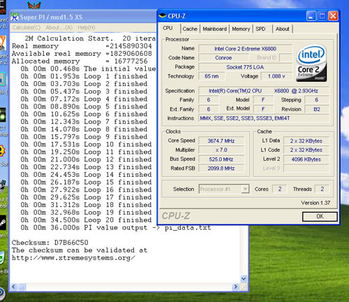
The overclock results are not a mistake. We managed to reach right at 4.0GHz with an X6800 at 1.575V. This represented the standard 11x ratio at a 1452 FSB. Even more spectacular was the reduced multiplier overclocking, where we reached a 2100 FSB (525 base) at a 7X multiplier AT DEFAULT VOLTAGE.


These results were with air cooling using a Tuniq 120 air cooler, which sandwiches a 120mm fan in a finned heatpipe core as pictured above.
 |
| Click to enlarge |
One of our X6800 processors reached 2100 FSB, confirming NVIDIA's claims of overclocking an X6800 in their labs to 2070 FSB. Not only did we reach 2100 FSB (525) at a 7X multiplier (3.675GHz), we managed to reach that speed at default voltage. The system has run at those settings for several days without incident and has handled every test and benchmark we have thrown at the system. However, it should also be pointed out that a second X6800 CPU would not overclock 1 MHz higher than 1900 FSB (450) on this same motherboard, even though that X6800 reached a similar 4GHz maximum overclock and similar "default voltage" overclocks.
We have yet to find anything obvious that would explain these differences in maximum FSB in the X6800 chips we tested. Revision and Stepping explained nothing, and we also had four retail E6600 we tested that would not reach above 1800 FSB. We are looking into these findings further and hope to find some explanations to share with you that will explain these maximum FSB differences among 4MB Cache Core 2 chips.
 |
| Click to enlarge |
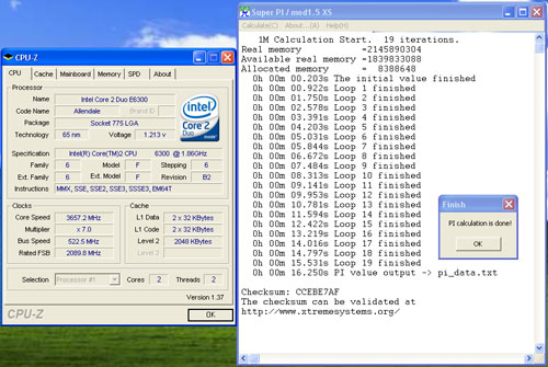
Interestingly, all of the 2MB cache Core 2 processors we tested reached at least 2000 FSB, with the two tested E6300 reaching 2100 FSB (522x7 and 6x525). We were prepared to call the amount of cache the defining difference in FSB performance until the late X6800 reached 2100 in our labs and NVIDIA confirmed their own 2070 results with an X6800 Extreme. We are much more confident that 2MB Cache chips can top 2000 FSB and we are very anxious to find something that will help you identify 4MB cache chips that will reach the "magic" 2000, 2070, and 2100 FSB overclocks.
Overall overclocking performance with the 680i was spectacular, and the results should excite any of you who want to do some serious overclocking with a Core 2 processor. At the very least the nForce 600i chipset family gives shoppers new choices in motherboards that will make the most of their Core 2 processor.


60 Comments
View All Comments
yyrkoon - Thursday, November 9, 2006 - link
From my little experience with an Asrock board that can use this program, it WILL adjust clock frequency on the fly, however I think that voltage changes need be done only by rebooting. Reguardless whether I'm remembering correctly, I'm fairly certain atleast one possible change needs to be done during, or after a reboot, could be thinking of clock multiplier maybe ?Pirks - Thursday, November 9, 2006 - link
that sucks. guess I'll have to wait till nVidia makes 100% nonreboot-OC mobo, or on-the-fly-OC mobo where you just click a couple of buttons in Windows and voila - your machine turns from quiet office machine to a Crysis fireball, and vice versa - I can dream, can't I? ;)ssiu - Wednesday, November 8, 2006 - link
Since NVIDIA claims the 680i has better FSB overclock than the 650i's, and the 680i results are on par with the mainstream P965's, I am afraid that the 650i's would be significantly worse than the DS3s/P5Bs. In other words, I am afraid that the 650i's are not really a new competitive option for budget/mainstream overclockers.yyrkoon - Wednesday, November 8, 2006 - link
I dont think any true enthusiast is going to be buying a mid range board(chipset) to begin with. If the Intel numbering shceme is anything like the AM2 numbering scheme, the 650i will probably have less availible PCI-E lanes as well, and would be a major factor in my personal decission in buying any such hardware, and I know I'm not alone ;)Jedi2155 - Wednesday, November 8, 2006 - link
I don't think your definition of enthusiast is wholly correct but rather the Manufacturer idea of enthusiasist. I personally think many enthusiasists do indeed have a limited budget, and after seeing the pricing of Asus 680i board, I think mid-range is the way to go...hoping for a cheap < $250 680i board >_>.yyrkoon - Wednesday, November 8, 2006 - link
Yeah, He wasnt talking about true enthusiasts though, I realize this after re-reading his post.One a side note, that if my board brand of choice suddenly went away (ABIT), I would seriously consider buying a Gigabyte board, but the DS3 doesnt seem to be making a lot of people happy in the stability category. What I'm trying to say here, is that perhaps the board MAY not OC as well, but that according to what I've read (reviews, forum posts, and A LOT of newegg user reviews), it couldnt do much worse than the Gigabyte board in this area.
The second question I'd be asking myself, is WHO THE HELL is EVGA . . . we all know they make Video cards (probably the best for customer support for nVidia products).
I'm definately interrested in the 680i chipset, but i think my brand of choice for MANY years now would remain the same, and that I'll be sticking with ABIT :)
Gary Key - Wednesday, November 8, 2006 - link
1. The reference board is designed and engineered by NVIDIA. Foxconn manufactures the boards for the "launch" partners that include BFG and others. Asus, Abit, DFI, Gigabyte, and others will have their custom designed boards out in a few weeks.2. The Abit board is very interesting, here is pic of it - http://img474.imageshack.us/img474/2044/in932xmaxy...">Abit 680i - ;)
yyrkoon - Thursday, November 9, 2006 - link
Didnt even know there was one this close to release gary, lol thanks for the link. Judging by the 5 SATAII connectors, previously released ABIT boards, and what LOOKS like an eSATA connector on the back panel, I suppose this board will support eSATA, and possibly a SATA PM ?Stele - Friday, November 10, 2006 - link
That Abit 680i board looks very interesting indeed... if nothing else because it looks like it sports a digital PWM power supply circuitry similar to that used by DFI in the latter's LANParty UT NF590 SLI-M2R motherboard (the Pulse PA1315NL coupled inductor array is a dead giveaway, as it is designed for use only with Volterra's VT11x5M digital PWM circuitry).Unfortunately more information on such circuitry is proving very difficult to find (Volterra themselves restrict their product details and datasheets to design partners only) ... it'd be great to know how such a power circuit compares in performance and capabilities over the traditional PWM-MOSFET-based ones.
Curiously, the Abit 680i seems to have dropped the AudioMax daughter board.
yyrkoon, I'm guessing the 5th SATA II and the eSATA port are there courtesy of an SiI3132 controller - which is likely the little square IC under the upper heatpipe, just beside the audio connector block. As such, the usual capabilities and features of the said IC would apply, I think :)
yyrkoon - Wednesday, November 8, 2006 - link
I'd just like ot point out that DualNet technology is NOT true NIC Teaming, or rather Link agrregation(802.11a/d I think).When I first heard about DualNet I was extremely excited, since I had been doing TONS of research on NIC bonding etc, but after doing some homework, I found that DuelNet only supports out going packets. It was my hope that you could link two of these boards via a regular GbE switch, and get instant 2GbE connections, but this is not the case(unless they've recently redone DualNet).
Now to the question: Since SATA port Multiplier HBAs require a specific SIL chip(s) on the device they communicate with (to give full speeds of a true RAID), what are the chances that nVidia boards will work with these devices ?
In the past, I've seen two AM2 boards that have a built in SIL chip with eSATA connectors on the board back panel (ABIT, and Asus), but onboard SIL 'chipsets' seem to be rather limited(as in only supporting PM support on two SATA connections). I'd personally REALLY like to see this technology standardized, so it doesnt matter WHAT SATA controller chipset you're using. I also think that once nVidia realizes that PM support onboard is a major plus, and once they implement it, they COULD be taken seriously by many Intel fans.
Also, some Intel chipset fans believe that Intel chipsets are best for a rock solid system (for the record, I'm not one of these people), I guess we'll see if nVidia will change thier minds.