More Mainstream DX10: AMD's 2400 and 2600 Series
by Derek Wilson on June 28, 2007 8:35 AM EST- Posted in
- GPUs
A Closer Look at RV610 and RV630
The RV6xx parts are similar to the R600 hardware we've already covered in detail. There are a few major differences between the two classes of hardware. First and foremost, the RV6xx GPUs include full video decode acceleration for MPEG-2, VC-1, and H.264 encoded content through AMD's UVD hardware. There was some confusion over this when R600 first launched, but AMD has since confirmed that UVD hardware is not at all present in their high end part.
We also have a difference in manufacturing process. R600 uses an 80nm TSMC process aimed at high speed transistors, while their RV610 and RV630 GPU based cards are fabbed on a 65nm TSMC process aimed at lower power consumption. The end result is that these GPUs will run much cooler and require much less power than their big brother the R600.
Transistor speed between these two processes ends up being similar in spite of the focus on power over performance at 65nm. RV610 is built with 180M transistors, while RV630 contains 390M. This is certainly down from the huge transistor count of R600, but nearly 400M is nothing to sneeze at.
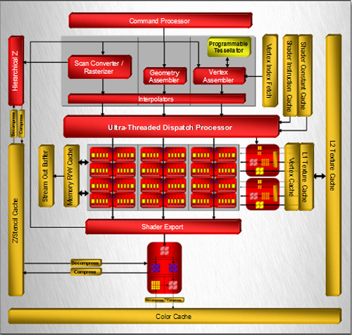
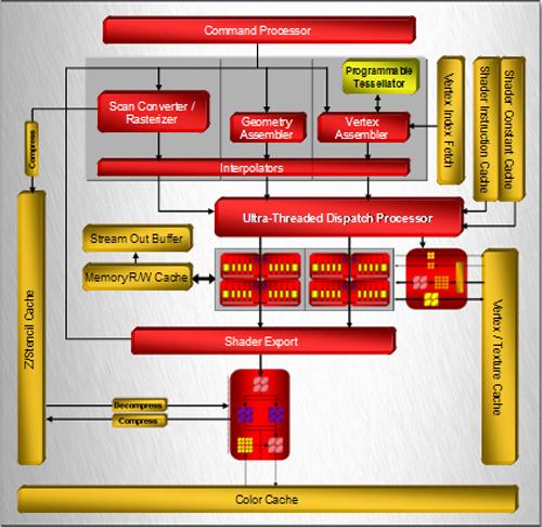
Aside from the obvious differences of transistor count and the number of different units (shaders, texture unit, etc.), the only other major difference is in memory bus width. All RV610 GPU based hardware will have a 64-bit memory bus, while RV630 based parts will feature a 128-bit connection to memory. Here's the layout of each GPU:

RV630 Block Diagram

RV610 Block Diagram
One of the first things that jump out is that both RV6xx based designs feature only one render back end block. This part of the chip is responsible for alpha (transparency) and fog, dealing with final z/stencil buffer operations, sending MSAA samples back up to the shader to be resolved, and ultimately blending fragments and writing out final pixel color. Maximum pixel fill rate is limited by the number of render back ends.
In the case of both current RV6xx GPUs, we can only draw out a maximum of 4 pixels per clock (or we can do 8 z/stencil-only ops per clock). While we don't expect extreme resolutions to be run on these parts (at least not in games), we could run into issues with effects that make heavy use of MRTs (multiple render targets), z/stencil buffers, and antialiasing. With the move to DX10, we expect developers to make use of the additional MRTs they have available, and lower resolutions benefit from AA more than high resolutions as well. We would really like to see higher pixel draw power here. Our performance tests will reflect the fact that AA is not kind to AMD's new parts, because of the lack of hardware resolve as well as the use of only one render back end.
Among the notable features that we will see here are tessellation, which could have an even larger impact on low end hardware for enabling detailed and realistic geometry, and CFAA filtering options. Unfortunately, we might not see that much initial use made of the tessellation hardware, and with the reduced pixel draw and shading power of the RVxx series, we are a little skeptical of the benefits of CFAA.
From here, lets move on and take a look at what we actually get in retail products.
The RV6xx parts are similar to the R600 hardware we've already covered in detail. There are a few major differences between the two classes of hardware. First and foremost, the RV6xx GPUs include full video decode acceleration for MPEG-2, VC-1, and H.264 encoded content through AMD's UVD hardware. There was some confusion over this when R600 first launched, but AMD has since confirmed that UVD hardware is not at all present in their high end part.
We also have a difference in manufacturing process. R600 uses an 80nm TSMC process aimed at high speed transistors, while their RV610 and RV630 GPU based cards are fabbed on a 65nm TSMC process aimed at lower power consumption. The end result is that these GPUs will run much cooler and require much less power than their big brother the R600.
Transistor speed between these two processes ends up being similar in spite of the focus on power over performance at 65nm. RV610 is built with 180M transistors, while RV630 contains 390M. This is certainly down from the huge transistor count of R600, but nearly 400M is nothing to sneeze at.
Aside from the obvious differences of transistor count and the number of different units (shaders, texture unit, etc.), the only other major difference is in memory bus width. All RV610 GPU based hardware will have a 64-bit memory bus, while RV630 based parts will feature a 128-bit connection to memory. Here's the layout of each GPU:


One of the first things that jump out is that both RV6xx based designs feature only one render back end block. This part of the chip is responsible for alpha (transparency) and fog, dealing with final z/stencil buffer operations, sending MSAA samples back up to the shader to be resolved, and ultimately blending fragments and writing out final pixel color. Maximum pixel fill rate is limited by the number of render back ends.
In the case of both current RV6xx GPUs, we can only draw out a maximum of 4 pixels per clock (or we can do 8 z/stencil-only ops per clock). While we don't expect extreme resolutions to be run on these parts (at least not in games), we could run into issues with effects that make heavy use of MRTs (multiple render targets), z/stencil buffers, and antialiasing. With the move to DX10, we expect developers to make use of the additional MRTs they have available, and lower resolutions benefit from AA more than high resolutions as well. We would really like to see higher pixel draw power here. Our performance tests will reflect the fact that AA is not kind to AMD's new parts, because of the lack of hardware resolve as well as the use of only one render back end.
Among the notable features that we will see here are tessellation, which could have an even larger impact on low end hardware for enabling detailed and realistic geometry, and CFAA filtering options. Unfortunately, we might not see that much initial use made of the tessellation hardware, and with the reduced pixel draw and shading power of the RVxx series, we are a little skeptical of the benefits of CFAA.
From here, lets move on and take a look at what we actually get in retail products.


96 Comments
View All Comments
Spoelie - Thursday, June 28, 2007 - link
think about the fact that the x1950xt has less transistors then a HD2600xt, and this is even more disappointingcoldpower27 - Thursday, June 28, 2007 - link
There just wasn't much choice, 390 Million for a midrange part on ATi's side that performs worse then Nvidia's 289 Million part, is quite a sorry state of affairs.It's too bad this generation was so expensive on the feature front that barely any transistor budget was left for implementing performance and were left with hardware that only performs marginally faster if that then the previous generation products.
I am quite disappointed that ATi parts are currently slower despite having a larger transistor budget and higher core clock.
TA152H - Thursday, June 28, 2007 - link
Maybe because they weren't designed for DX9 performance, to state the obvious. They are DX10 parts, and should be judged on how well they perform on that.Shintai - Thursday, June 28, 2007 - link
DX10 sucks on both 8600GT/S and 2600XT, unless playing at 5-8FPS is you.2900XT/8800GTS/X is needed for DX10. And better yet, SLI/CF or the next generation.
DX10 on these midrange nVidia and AMD GPUs is 100% useless.
And for what reason do you think they will perform magically better in DX10? 2900XT didnt over 8800. And there is no reason on why it should be better.
TA152H - Thursday, June 28, 2007 - link
Another person that can't read.I didn't say it would perform better, or worse. We'll see how well it performs when they do the proper tests. Until then, stop the whining. Afterwards, if it sucks, I'll whine with you.
Shintai - Thursday, June 28, 2007 - link
Just read some of the other sites that tested DX10.Le Québécois - Thursday, June 28, 2007 - link
From what I know, all DX10 games or applications out there right now were developed for DX9 and received DX10 feature as an after thought. For REAL DX10 we will have to wait for Crysis.titan7 - Saturday, June 30, 2007 - link
Company of Heroes was designed for d3d10 from the start. It's as much a real d3d10 game as crysis will be.coldpower27 - Thursday, June 28, 2007 - link
There won't be any "REAL" DX10 for sometime to come, oit takes ages to develop native API games.swaaye - Thursday, June 28, 2007 - link
I've seen Crysis on a 8800GTX. Don't expect to play it well on less, unless the game devs perform some serious miracles. And I wouldn't bet one that. :)