AMD Reveals More Llano Details at ISSCC: 32nm, Power Gating, 4-cores, Turbo?
by Anand Lal Shimpi on February 8, 2010 12:00 AM EST- Posted in
- CPUs
After cashing Intel’s check and appearing more competitive than expected against Clarkdale 2010 is like a fresh start for AMD. The news gets better.
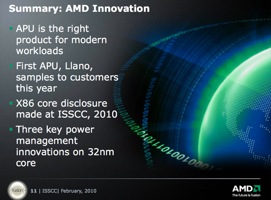
Late last year AMD said that before the end of 2010 it would be sampling its first APU (Accelerated Processing Unit) - codenamed Llano. Today AMD is announcing that the first Llano samples, built on Global Foundries 32nm high-k + metal gate, SOI process will be sampling to partners in the first half of this year.
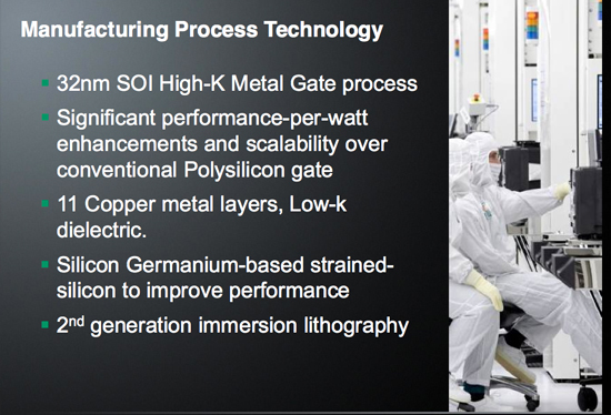
GF's 32nm SOI High-K + MG process will be used with Llano
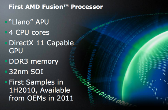
For those not in the know, Llano is AMD’s first hybrid CPU-GPU with on-die graphics. The graphics core is a derivative of AMD’s DirectX 11 Evergreen lineup (the same lineage as the Radeon HD 5970, 5870, 5850, 5670, 5570, 5450, etc...).
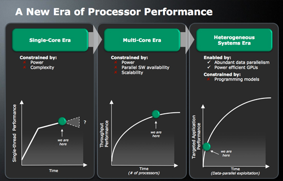
Llano will go up against Sandy Bridge, which seems to have been pushed back to 2011 for volume availability according to Intel’s internal roadmaps. While Sandy Bridge will have graphics on-die, it will still only be DX10 class - AMD will have the feature-set advantage as far as graphics is concerned.

Llano's Features
Today we learn a bit more about the CPU side of Llano. The first chip will be a quad-core processor plus on-die graphics. Each core is Phenom II derived, but there’s no shared L3 cache. So Llano cores look a lot like Athlon II cores. I’m hearing that they may have some architectural tweaks, so performance could be better than present-day Athlon IIs.
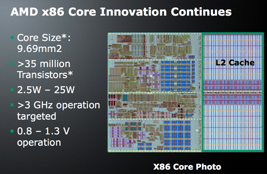
At 32nm each core (minus L2 cache) is only 9.69 mm^2 and is made up of over 35M transistors. Each core is paired with its own 1MB L2 cache, meaning the quad-core processor will have a total of 4MB of L2 on-die. AMD expects Llano to run at above 3GHz, which should be more than possible at 32nm given that we’re already at close to 3GHz with the 45nm Athlon II X4.
AMD’s First Power Gated CPU
With Nehalem Intel introduced power gating, a technique that allows a core to be near-completely powered down minimizing leakage current when inactive. This not only reduces idle power but it also enables Intel to use extra TDP to turbo up active cores.
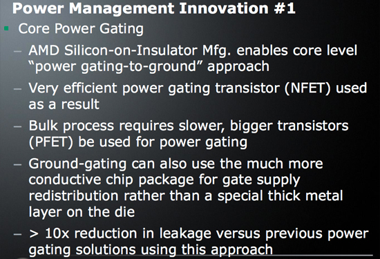
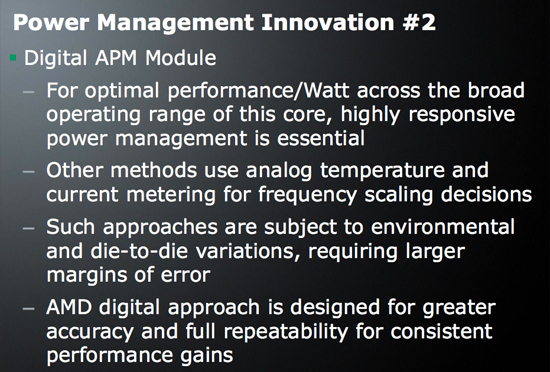
Llano uses power gating as well as a Digital APM Module. AMD doesn’t go into much detail on the digital APM module but I’m guessing we’ll see the same sort of turbo-like functionality out of Llano, including graphics turbo.
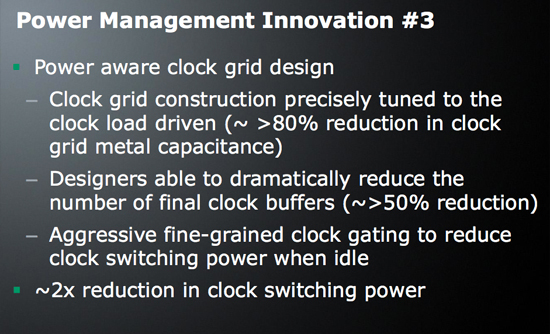
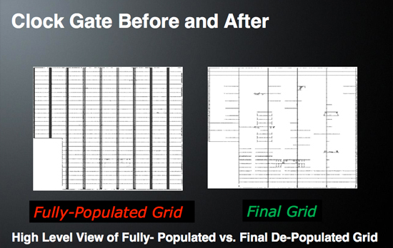
AMD also pointed out that Llano uses a “power aware clock grid design”. I couldn’t get much more information out of AMD on this one, other than its expecting a ~2x reduction in clock switching power. Simply distributing the clock to all parts of a modern day microprocessor can take up quite a bit of power, any improvements in efficiency there are very important.
I’ll keep digging to see if I can get any more details on this aspect of Llano.
Final Words
Llano will obviously require a new socket. All AMD is saying is that OEMs will be shipping systems in 2011. It’s unclear if we’ll see anything in the channel before then, but with sampling in the coming months it appears that AMD could be ready for Sandy Bridge when it arrives next year.
AMD isn’t qualifying its 2011 statement with an indication of what quarter to expect systems. Given that the first samples are going out now, I’d expect to see Llano sometime in the first half of 2011 but that’s purely conjecture on my part. Sandy Bridge is scheduled to ship in volume in the first quarter of 2011.
The big questions going forward are 1) how much AMD and Intel are going to scale up its graphics performance on these chips, and 2) how important DX11 support will be to the upcoming APU race.


58 Comments
View All Comments
techwriters4breakfast - Monday, February 8, 2010 - link
went to this cpu article with anand as the usual author,then read first phrase: "After cashing Intel’s check..."
i was prepared for some intel propaganda hehe.
acejj26 - Monday, February 8, 2010 - link
Does no one edit slides before they publish them? "Across the broad?" Shouldn't PR slides go through several editors before being made public?jjjpflynn - Tuesday, February 9, 2010 - link
Perhaps you should read more carefully."...across the broad operating range of this core..."
Nothing wrong with it at all.
UNHchabo - Monday, February 8, 2010 - link
The sentence involved the phrase "...across the broad operating range..."I can see why you thought the line ended there though.
Kibbles - Monday, February 8, 2010 - link
In that X ray, can you tell where the CPU/GPU are?Kiijibari - Monday, February 8, 2010 - link
NOO, because it is just a plot of the x86 core ... it says so on the picture ...Kibbles - Monday, February 8, 2010 - link
so that's one single core?Calin - Tuesday, February 9, 2010 - link
Yes, one single core.The final processor will have four of those (each core includes L2 cache), then some "glue" logic, memory controller and so on, then the graphic unit.
Hiravaxis - Monday, February 8, 2010 - link
I don't think DirectX 11 is of much value to a first iteration CPU/GPU integration like this.The GPU won't be powerful enough to take advantage of any of the Dx11 functions, so it's really just a check box for AMD.
But kudos to them if they can get this out to compete with Sandy Bridge!
tcube - Saturday, March 20, 2010 - link
just do the math man... this is NOT bulk we're talking about this is SOI/HkMg ... that means you will get it in 3ghz flavours, meaning it can push about 2TFLOPS at that horrendous power it is an equal match to todays descretes. Think: 4x the speed, 32 nm vs 40 nm, think much denser SOI vs bulk process.(provided it will not have less then 4x less rops then HD5870) This baby is going to play crysis like a charm.... not to mention new games. All this provided this thing is not going to be memory starved! So hell yeah! Give me 4 laned 2ghz DDR3 and I won't need a discrete any longer! This thing will prove or fail depending on io it will have... let's pray amd gets the balance right this time around! And let's pray we get a SOI incarnation for the HD5870 as the next generation...