Original Link: https://www.anandtech.com/show/5699/nvidia-geforce-gtx-680-review
NVIDIA GeForce GTX 680 Review: Retaking The Performance Crown
by Ryan Smith on March 22, 2012 9:00 AM EST“How do you follow up on Fermi?” That’s the question we had going into NVIDIA’s press briefing for the GeForce GTX 680 and the Kepler architecture earlier this month. With Fermi NVIDIA not only captured the performance crown for gaming, but they managed to further build on their success in the professional markets with Tesla and Quadro. Though it was a very clearly a rough start for NVIDIA, Fermi ended up doing quite well in the end.
So how do you follow up on Fermi? As it turns out, you follow it up with something that is in many ways more of the same. With a focus on efficiency, NVIDIA has stripped Fermi down to the core and then built it back up again; reducing power consumption and die size alike, all while maintaining most of the aspects we’ve come to know with Fermi. The end result of which is NVIDIA’s next generation GPU architecture: Kepler.
Launching today is the GeForce GTX 680, at the heart of which is NVIDIA’s new GK104 GPU, based on their equally new Kepler architecture. As we’ll see, not only has NVIDIA retaken the performance crown with the GeForce GTX 680, but they have done so in a manner truly befitting of their drive for efficiency.
| GTX 680 | GTX 580 | GTX 560 Ti | GTX 480 | |
| Stream Processors | 1536 | 512 | 384 | 480 |
| Texture Units | 128 | 64 | 64 | 60 |
| ROPs | 32 | 48 | 32 | 48 |
| Core Clock | 1006MHz | 772MHz | 822MHz | 700MHz |
| Shader Clock | N/A | 1544MHz | 1644MHz | 1401MHz |
| Boost Clock | 1058MHz | N/A | N/A | N/A |
| Memory Clock | 6.008GHz GDDR5 | 4.008GHz GDDR5 | 4.008GHz GDDR5 | 3.696GHz GDDR5 |
| Memory Bus Width | 256-bit | 384-bit | 256-bit | 384-bit |
| Frame Buffer | 2GB | 1.5GB | 1GB | 1.5GB |
| FP64 | 1/24 FP32 | 1/8 FP32 | 1/12 FP32 | 1/12 FP32 |
| TDP | 195W | 244W | 170W | 250W |
| Transistor Count | 3.5B | 3B | 1.95B | 3B |
| Manufacturing Process | TSMC 28nm | TSMC 40nm | TSMC 40nm | TSMC 40nm |
| Launch Price | $499 | $499 | $249 | $499 |
Technically speaking Kepler’s launch today is a double launch. On the desktop we have the GTX 680, based on the GK104 GPU. Meanwhile in the mobile space we have the GT640M, which is based on the GK107 GPU. While NVIDIA is not like AMD in that they don’t announce products ahead of time, it’s a sure bet that we’ll eventually see GK107 move up to the desktop and GK104 move down to laptops in the future.
What you won’t find today however – and in a significant departure from NVIDIA’s previous launches – is Big Kepler. Since the days of the G80, NVIDIA has always produced a large 500mm2+ GPU to serve both as a flagship GPU for their consumer lines and the fundamental GPU for their Quadro and Tesla lines, and have always launched with that big GPU first. At 294mm2 GK104 is not Big Kepler, and while NVIDIA doesn’t comment on unannounced products, somewhere in the bowels of NVIDIA Big Kepler certainly lives, waiting for its day in the sun. As such this is the first NVIDIA launch where we’re not in a position to talk about the ramifications for Tesla or Quadro, or really for that matter what NVIDIA’s peak performance for this generation might be.
Anyhow, we’ll jump into the full architectural details of GK104 in a bit, but let’s quickly talk about the specs first. Unlike Fermi or AMD’s GCN, Kepler is not a brand new architecture. To be sure there are some very important changes, but at a high level the workings of Kepler have not significantly changed compared to Fermi. With Kepler what we’re ultimately looking at is a die shrunk distillation of Fermi, and in the case of GK104 that’s specifically a distillation of GF114 rather than GF110.
Starting from the top, GTX 680 features a fully enabled GK104 GPU – unlike the first generation of Fermi products there are no shenanigans with disabled units here. This means GTX 680 has 1536 CUDA cores, a massive increase from GTX 580 (512) and GTX 560 Ti (384). Note however that NVIDIA has dropped the shader clock with Kepler, opting instead to double the number of CUDA cores to achieve the same effect, so while 1536 CUDA cores is a big number it’s really only twice the number of cores of GF114 as far as performance is concerned. Joining those 1536 CUDA cores are 32 ROPs and 128 texture units; the number of ROPs is effectively unchanged from GF114, while the number of texture units has been doubled. Meanwhile on the memory and cache side of things GTX 680 features a 256-bit memory bus coupled with 512KB of L2 cache.
As for clockspeeds, GTX 680 will introduce a few wrinkles courtesy of Kepler. As we mentioned before, the shader clock is gone in Kepler, with everything now running off of the core clock (or as NVIDIA likes to put it, the graphics clock). At the same time Kepler introduces the Boost Clock – effectively a turbo clock for the GPU – so we still have a 3rd clock to pay attention to. With that said, GTX 680 ships at a base clock of 1006MHz and a boost clock of 1058MHz. On the memory side of things NVIDIA has finally managed to fully hammer out their memory controller, allowing NVIDIA to ship with a memory clock of 6.006GHz.
Taken altogether, on paper GTX 680 has roughly 195% the shader performance, 260% the texture performance, 87% of the ROP performance, and 100% of the memory bandwidth of GTX 580. Or as compared to its more direct ancestor the GTX 560 Ti, GTX 680 has 244% of the shader performance, 244% of the texture performance, 122% of the ROP performance, and 150% of the memory bandwidth of GTX 560 Ti. Compared to GTX 560 Ti NVIDIA has effectively doubled every aspect of their GPU except for ROP performance, which is the one area where NVIDIA believes they already have enough performance.
On the power front, GTX 680 has a few different numbers to contend with. NVIDIA’s official TDP is 195W, though as with the GTX 500 series they still consider this is an average number rather than a true maximum. The second number is the boost target, which is the highest power level that GPU Boost will turbo to; that number is 170W. Finally, while NVIDIA doesn’t publish an official idle TDP, the GTX 680 should have an idle TDP of around 15W. Overall GTX 680 is targeted at a power envelope somewhere between GTX 560 Ti and GTX 580, though it’s closer to the former than the latter.
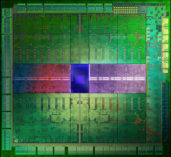
As for GK104 itself, as we’ve already mentioned GK104 is a smaller than average GPU for NVIDIA, with a die size of 294mm2. This is roughly 89% the size of GF114, or compared to GF110 a mere 56% of the size. Inside that 294mm2 NVIDIA packs 3.5B transistors thanks to TSMC’s 28nm process, only 500M more than GF110 and largely explaining why GK104 is so small compared to GF110. Or to once again make a comparison to GF114, this is 1050M (53%) more than GF114, which makes the fact that GK104 doubles most of GF114’s functional units all the more surprising. With Kepler NVIDIA is going to be heavily focusing on efficiency, and this is one such example of Kepler’s efficiency in action.
Last but not least, let’s talk about pricing and availability. GTX 680 is the successor to GTX 580 and NVIDIA will be pricing it accordingly, with an MSRP of $500. This is the same price that the GTX 580 and GTX 480 launched at back in 2010, and while it’s consistent for an x80 video card it’s effectively a conservative price given GK104’s die size. NVIDIA does need to bring their pricing in at the right point to combat AMD, but they’re in no more of a hurry than AMD to start any price wars, so it’s conservative pricing all around for the time being.
AMD’s competition of course is the recently launched Radeon HD 7970 and 7950. Priced at $550 and $450, the GTX 680 sits right in between them in terms of pricing. However with regard to gaming performance the GTX 680 is generally more than a match for the 7970, which is going to leave AMD in a tough spot. AMD’s partners do have factory overclocked cards, but those only close the performance gap at the cost of an even wider price gap. NVIDIA has priced the GTX 680 to undercut the 7970, and that’s exactly what will be happening today.
As for availability, we’re told that it should be similar to past high end video card launches, which is to say it will be touch and go. As with any launch NVIDIA has been stockpiling cards but it’s still a safe bet that GTX 680 will sell out in the first day. Beyond the initial launch it’s not clear whether NVIDIA will be able to keep up with demand over the next month or so. NVIDIA has been fairly forthcoming to their investors about how 28nm production is going, and while yields have been acceptable TSMC doesn’t have enough wafers to satisfy all of their customers at once, so NVIDIA is still getting fewer wafers than they’d like. Until very recently AMD’s partners have had a difficult time keeping the 7970 in stock, and it’s likely it will be the same story for NVIDIA’s partners.
The Kepler Architecture: Fermi Distilled
As GPU complexity has increased over the years, so has the amount of time it takes to design a GPU. Specific definitions vary on what constitutes planning, but with modern GPUs such as Fermi, Kepler, and Tahiti planning basically starts 4+ years ahead of time. At this point in time GPUs have a similarly long development period as CPUs, and that alone comes with some ramifications.
The biggest ramification of this style of planning is that because designing a GPU is such a big undertaking, it’s not something you want to do frequently. In the CPU space Intel has their tick-tock strategy, which has Intel making incremental architecture updates every 2 years. While in the GPU space neither NVIDIA or AMD have something quite like that – new architectures and new process nodes still tend to premiere together – there is a similar need to spread out architectures over multiple years.
For NVIDIA, Kepler is the embodiment of that concept. Kepler brings with it some very important architectural changes compared to Fermi, but at the same time it’s still undeniably Fermi. From a high level overview Kepler is identical to Fermi: it’s still organized into CUDA cores, SMs, and GPCs, and how warps are executed has not significantly changed. Nor for that matter has the rendering side significantly changed, with rendering still being handled in a distributed fashion through raster engines, polymorph engines, and of course the ROPs. The fact that NVIDIA has chosen to draw up Kepler like Fermi is no accident or coincidence; at the end of the day Kepler is the next generation of Fermi, tweaked and distilled to improve on Fermi’s strengths while correcting its weaknesses.
For our look at Kepler’s architecture, we’re going to be primarily comparing it to GF114, aka Fermi Lite. As you may recall, with Fermi NVIDIA had two designs: a multipurpose architecture for gaming and graphics (GF100/GF110), and a streamlined architecture built with a stronger emphasis on graphics than compute (GF104, etc) that was best suited for use in consumer graphics. As hinted at by the name alone, GK104 is designed to fill the same consumer graphics role as GF114, and consequently NVIDIA built GK104 off of GF114 rather than GF110.
So what does GK104 bring to the table? Perhaps it’s best to start with the SMs, as that’s where most of the major changes have happened.
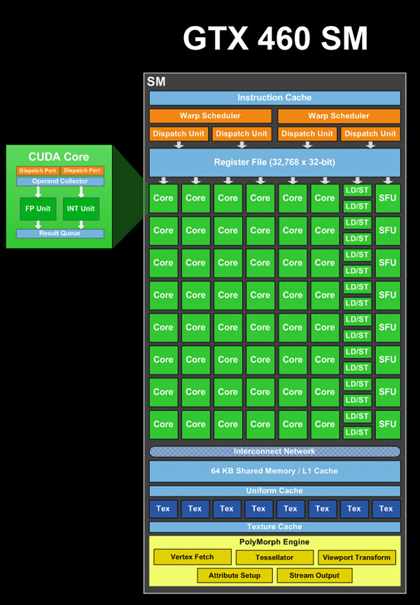
In GF114 each SM contained 48 CUDA cores, with the 48 cores organized into 3 groups of 16. Joining those 3 groups of CUDA cores were 16 load/store units, 16 interpolation SFUs, 8 special function SFUs, and 8 texture units. Feeding all of those blocks was a pair of warp schedulers, each of which could issue up to 2 instructions per core clock cycle, for a total of up to 4 instructions in flight at any given time.
GF104/GF114 SM Functional Units
- 16 CUDA cores (#1)
- 16 CUDA cores (#2)
- 16 CUDA cores, FP64 capable (#3)
- 16 Load/Store Units
- 16 Interpolation SFUs (not on NVIDIA's diagrams)
- 8 Special Function SFUs
- 8 Texture Units
Within the SM itself different units operated on different clocks, with the schedulers and texture units operating on the core clock, while the CUDA cores, load/store units, and SFUs operated on the shader clock, which ran at twice the core clock. As NVIDIA’s warp size is 32 threads, if you do the quick math you realize that warps are twice as large as any block of functional units, which is where the shader clock comes in. With Fermi, a warp would be split up and executed over 2 cycles of the shader clock; 16 threads would go first, and then the other 16 threads over the next clock. The shader clock is what allowed NVIDIA to execute a full warp over a single graphics clock cycle while only using enough hardware for half of a warp.
So how does GK104 change this? The single most important aspect of GK104, the thing that in turn dictates the design of everything else, is that NVIDIA has dropped the shader clock. Now the entire chip, from ROP to CUDA core, runs on the same core clock. As a consequence, rather than executing two half-warps in quick succession GK104 is built to execute a whole warp at once, and GK104’s hardware has changed dramatically as a result.
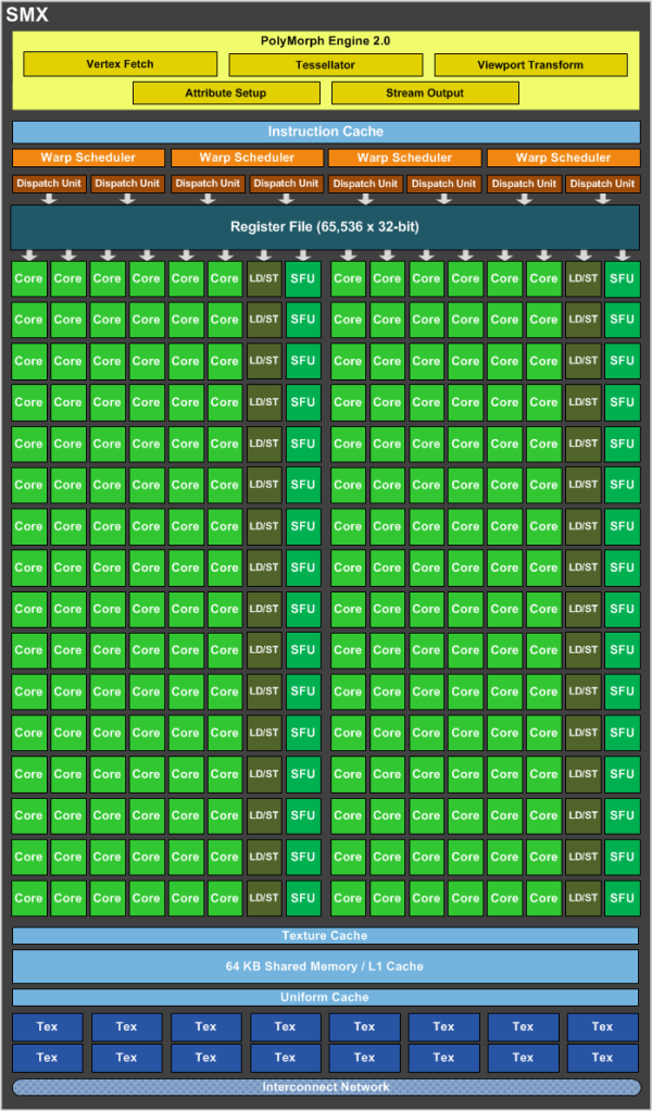
Because NVIDIA has essentially traded a fewer number of higher clocked units for a larger number of lower clocked units, NVIDIA had to go in and double the size of each functional unit inside their SM. Whereas a block of 16 CUDA cores would do when there was a shader clock, now a full 32 CUDA cores are necessary. The same is true for the load/store units and the special function units, all of which have been doubled in size in order to adjust for the lack of a shader clock. Consequently, this is why we can’t just immediately compare the CUDA core count of GK104 and GF114 and call GK104 4 times as powerful; half of that additional hardware is just to make up for the lack of a shader clock.
But of course NVIDIA didn’t stop there, as swapping out the shader clock for larger functional units only gives us the same throughput in the end. After doubling the size of the functional units in a SM, NVIDIA then doubled the number of functional units in each SM in order to grow the performance of the SM itself. 3 groups of CUDA cores became 6 groups of CUDA cores, 2 groups of load/store units, 16 texture units, etc. At the same time, with twice as many functional units NVIDIA also doubled the other execution resources, with 2 warp schedulers becoming 4 warp schedulers, and the register file being doubled from 32K entries to 64K entries.
Ultimately where the doubling of the size of the functional units allowed NVIDIA to drop the shader clock, it’s the second doubling of resources that makes GK104 much more powerful than GF114. The SMX is in nearly every significant way twice as powerful as a GF114 SM. At the end of the day NVIDIA already had a strong architecture in Fermi, so with Kepler they’ve gone and done the most logical thing to improve their performance: they’ve simply doubled Fermi.
Altogether the SMX now has 15 functional units that the warp schedulers can call on. Each of the 4 schedulers in turn can issue up to 2 instructions per clock if there’s ILP to be extracted from their respective warps, allowing the schedulers as a whole to issue instructions to up to 8 of the 15 functional units in any clock cycle.
GK104 SMX Functional Units
- 32 CUDA cores (#1)
- 32 CUDA cores (#2)
- 32 CUDA cores (#3)
- 32 CUDA cores (#4)
- 32 CUDA cores (#5)
- 32 CUDA cores (#6)
- 16 Load/Store Units (#1)
- 16 Load/Store Units (#2)
- 16 Interpolation SFUs (#1)
- 16 Interpolation SFUs (#2)
- 16 Special Function SFUs (#1)
- 16 Special Function SFUs (#2)
- 8 Texture Units (#1)
- 8 Texture Units (#2)
- 8 CUDA FP64 cores
While that covers the operation of the SMX in a nutshell, there are a couple of other things relating to the SMX that need to be touched upon. Because NVIDIA still only has a single Polymorph Engine per SMX, the number of Polymorph Engines hasn’t been doubled like most of the other hardware in an SMX. Instead the capabilities of the Polymorph Engine itself have been doubled, making each Polymorph Engine 2.0 twice as powerful as a GF114 Polymorph Engine. In absolute terms, this means each Polymorph Engine can now spit out a polygon in 2 cycles, versus 4 cycles on GF114, for a total of 4 polygons/clock across GK104.
The other change coming from GF114 is the mysterious block #15, the CUDA FP64 block. In order to conserve die space while still offering FP64 capabilities on GF114, NVIDIA only made one of the three CUDA core blocks FP64 capable. In turn that block of CUDA cores could execute FP64 instructions at a rate of ¼ FP32 performance, which gave the SM a total FP64 throughput rate of 1/12th FP32. In GK104 none of the regular CUDA core blocks are FP64 capable; in its place we have what we’re calling the CUDA FP64 block.
The CUDA FP64 block contains 8 special CUDA cores that are not part of the general CUDA core count and are not in any of NVIDIA’s diagrams. These CUDA cores can only do and are only used for FP64 math. What's more, the CUDA FP64 block has a very special execution rate: 1/1 FP32. With only 8 CUDA cores in this block it takes NVIDIA 4 cycles to execute a whole warp, but each quarter of the warp is done at full speed as opposed to ½, ¼, or any other fractional speed that previous architectures have operated at. Altogether GK104’s FP64 performance is very low at only 1/24 FP32 (1/6 * ¼), but the mere existence of the CUDA FP64 block is quite interesting because it’s the very first time we’ve seen 1/1 FP32 execution speed. Big Kepler may not end up resembling GK104, but if it does then it may be an extremely potent FP64 processor if it’s built out of CUDA FP64 blocks.
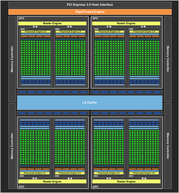
Moving on, now that we’ve dissected GK104’s SMX, let’s take a look at the bigger picture. Above the SM(X)es we have the GPCs. The GPCs contain multiple SMs and more importantly the Raster Engine responsible for all rasterization. As with the many other things being doubled in GK104, the number of GPCs has been doubled from 2 to 4, thereby doubling the number of Raster Engines present. This in turn changes the GPC-to-SM(X) ratio from 1:4 on GF114 to 1:2 on GK104. The ratio itself is not particularly important, but it’s worth noting that it does take more work for NVIDIA to lay down and connect 4 GPCs than it does 2 GPCs.
Last, but certainly not least is the complete picture. The 4 GPCs are combined with the rest of the hardware that makes GK104 tick, including the ROPs, the memory interfaces, and the PCIe interface. The ROPs themselves are virtually identical to those found on GF114; theoretical performance is the same, and at a lower level the only notable changes are an incremental increase in compression efficiency, and improved polygon merging. Similarly, the organization of the ROPs has not changed either, as the ROPs are still broken up into 4 blocks of 8, with each ROP block tied to a 64 bit memory controller and 128KB of L2 cache. Altogether there are 32 ROPs, giving us 512KB of L2 cache and a 256bit memory bus.
On a final tangent, the memory controllers ended up being an unexpected achievement for NVIDIA. As you may recall, Fermi’s memory controllers simply never reached their intended targets – NVIDIA hasn’t told us what those targets were, but ultimately Fermi was meant to reach memory clocks higher than 4GHz. With GK104 NVIDIA has improved their memory controllers and then some. GK104’s memory controllers can clock some 50% higher than GF114’s, leading to GTX 680 shipping at 6GHz.
On a technical level, getting to 6GHz is hard, really hard. GDDR5 RAM can reach 7GHz and beyond on the right voltage, but memory controllers and the memory bus are another story. As we have mentioned a couple of times before, the memory bus tends to give out long before anything else does, which is what’s keeping actual shipping memory speeds well below 7GHz. With GK104 NVIDIA’s engineers managed to put together a chip and board that are good enough to run at 6GHz, and this alone is quite remarkable given how long GDDR5 has dogged NVIDIA and AMD.
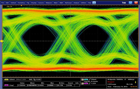
GK104 GDDR5 Signal Analysis
Perhaps the icing on the cake for NVIDIA though is how many revisions it took them to get to 6GHz: one. NVIDIA was able to get 6GHz on the very first revision of GK104, which after Fermi’s lackluster performance is a remarkable turn of events. And ultimately while NVIDIA says that they’re most proud of the end result of GK104, the fact of the matter is that everyone seems just a bit prouder of their memory controller, and for good reason.
The Kepler Architecture: Efficiency & Scheduling
So far we’ve covered how NVIDIA has improved upon Fermi for; now let’s talk about why.
Mentioned quickly in our introduction, NVIDIA’s big push with Kepler is efficiency. Of course Kepler needs to be faster (it always needs to be faster), but at the same time the market is making a gradual shift towards higher efficiency products. On the desktop side of matters GPUs have more or less reached their limits as far as total power consumption goes, while in the mobile space products such as Ultrabooks demand GPUs that can match the low power consumption and heat dissipation levels these devices were built around. And while strictly speaking NVIDIA’s GPUs haven’t been inefficient, AMD has held an edge on performance per mm2 for quite some time, so there’s clear room for improvement.
In keeping with that ideal, for Kepler NVIDIA has chosen to focus on ways they can improve Fermi’s efficiency. As NVIDIA's VP of GPU Engineering, Jonah Alben puts it, “[we’ve] already built it, now let's build it better.”
There are numerous small changes in Kepler that reflect that goal, but of course the biggest change there was the removal of the shader clock in favor of wider functional units in order to execute a whole warp over a single clock cycle. The rationale for which is actually rather straightforward: a shader clock made sense when clockspeeds were low and die space was at a premium, but now with increasingly small fabrication processes this has flipped. As we have become familiar with in the CPU space over the last decade, higher clockspeeds become increasingly expensive until you reach a point where they’re too expensive – a point where just distributing that clock takes a fair bit of power on its own, not to mention the difficulty and expense of building functional units that will operate at those speeds.
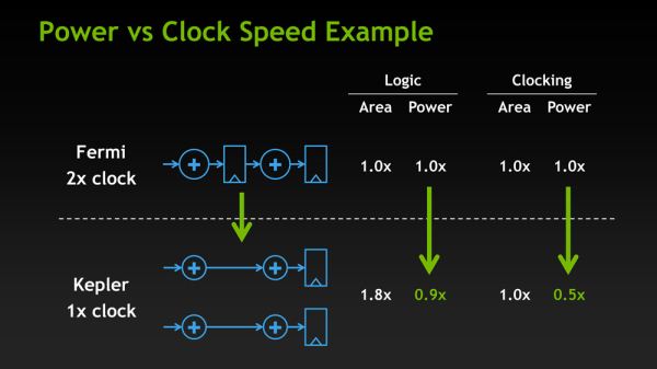
With Kepler the cost of having a shader clock has finally become too much, leading NVIDIA to make the shift to a single clock. By NVIDIA’s own numbers, Kepler’s design shift saves power even if NVIDIA has to operate functional units that are twice as large. 2 Kepler CUDA cores consume 90% of the power of a single Fermi CUDA core, while the reduction in power consumption for the clock itself is far more dramatic, with clock power consumption having been reduced by 50%.
Of course as NVIDIA’s own slide clearly points out, this is a true tradeoff. NVIDIA gains on power efficiency, but they lose on area efficiency as 2 Kepler CUDA cores take up more space than a single Fermi CUDA core even though the individual Kepler CUDA cores are smaller. So how did NVIDIA pay for their new die size penalty?
Obviously 28nm plays a significant part of that, but even then the reduction in feature size from moving to TSMC’s 28nm process is less than 50%; this isn’t enough to pack 1536 CUDA cores into less space than what previously held 384. As it turns out not only did NVIDIA need to work on power efficiency to make Kepler work, but they needed to work on area efficiency. There are a few small design choices that save space, such as using 8 SMXes instead of 16 smaller SMXes, but along with dropping the shader clock NVIDIA made one other change to improve both power and area efficiency: scheduling.
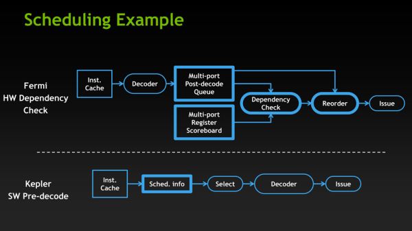
GF114, owing to its heritage as a compute GPU, had a rather complex scheduler. Fermi GPUs not only did basic scheduling in hardware such as register scoreboarding (keeping track of warps waiting on memory accesses and other long latency operations) and choosing the next warp from the pool to execute, but Fermi was also responsible for scheduling instructions within the warps themselves. While hardware scheduling of this nature is not difficult, it is relatively expensive on both a power and area efficiency basis as it requires implementing a complex hardware block to do dependency checking and prevent other types of data hazards. And since GK104 was to have 32 of these complex hardware schedulers, the scheduling system was reevaluated based on area and power efficiency, and eventually stripped down.
The end result is an interesting one, if only because by conventional standards it’s going in reverse. With GK104 NVIDIA is going back to static scheduling. Traditionally, processors have started with static scheduling and then moved to hardware scheduling as both software and hardware complexity has increased. Hardware instruction scheduling allows the processor to schedule instructions in the most efficient manner in real time as conditions permit, as opposed to strictly following the order of the code itself regardless of the code’s efficiency. This in turn improves the performance of the processor.
However based on their own internal research and simulations, in their search for efficiency NVIDIA found that hardware scheduling was consuming a fair bit of power and area for few benefits. In particular, since Kepler’s math pipeline has a fixed latency, hardware scheduling of the instruction inside of a warp was redundant since the compiler already knew the latency of each math instruction it issued. So NVIDIA has replaced Fermi’s complex scheduler with a far simpler scheduler that still uses scoreboarding and other methods for inter-warp scheduling, but moves the scheduling of instructions in a warp into NVIDIA’s compiler. In essence it’s a return to static scheduling.
Ultimately it remains to be seen just what the impact of this move will be. Hardware scheduling makes all the sense in the world for complex compute applications, which is a big reason why Fermi had hardware scheduling in the first place, and for that matter why AMD moved to hardware scheduling with GCN. At the same time however when it comes to graphics workloads even complex shader programs are simple relative to complex compute applications, so it’s not at all clear that this will have a significant impact on graphics performance, and indeed if it did have a significant impact on graphics performance we can’t imagine NVIDIA would go this way.
What is clear at this time though is that NVIDIA is pitching GTX 680 specifically for consumer graphics while downplaying compute, which says a lot right there. Given their call for efficiency and how some of Fermi’s compute capabilities were already stripped for GF114, this does read like an attempt to further strip compute capabilities from their consumer GPUs in order to boost efficiency. Amusingly, whereas AMD seems to have moved closer to Fermi with GCN by adding compute performance, NVIDIA seems to have moved closer to Cayman with Kepler by taking it away.
With that said, in discussing Kepler with NVIDIA’s Jonah Alben, one thing that was made clear is that NVIDIA does consider this the better way to go. They’re pleased with the performance and efficiency they’re getting out of software scheduling, going so far to say that had they known what they know now about software versus hardware scheduling, they would have done Fermi differently. But whether this only applies to consumer GPUs or if it will apply to Big Kepler too remains to be seen.
GPU Boost: Turbo For GPUs
Now that we’ve had a chance to take a look at the Kepler architecture, let’s jump into features. We’ll start with the feature that’s going to have the biggest impact on performance: GPU Boost.
Much like we’ve seen with CPUs in previous years, GPUs are reaching a point where performance is being limited by overall power consumption. Until the last couple of years GPU power consumption has been allowed to slowly drift up with each generation, allowing for performance to scale to an incredible degree. However for many of the same reasons NVIDIA has been focusing on efficiency in general, GPUs are being pressured to do more without consuming more.
The problem of course is compounded by the fact that there are a wide range of possible workloads for a GPU, much like there is for a CPU. With the need to design video cards around specific TDPs for both power supply and heat dissipation reasons, the goal becomes one of maximizing your performance inside of your assigned TDP.
The answer to that problem in the CPU space is turbo boosting – that is increasing the clockspeed of one or more CPU cores so long as the chip as a whole remains at or under its TDP. By using turbo, Intel and AMD have been able to both maximize the performance of lightly threaded applications by boosting a handful of cores to high speeds, and at the same time maximize heavily threaded performance by boosting a large number of cores by little to none. For virtually any CPU-bound workload the CPU can put itself into a state where the appropriate execution units are making the most of their TDP allocation.
Of course in the GPU world things aren’t that simple – for starters we don’t have a good analogy for a lightly threaded workload – but the concept is similar. GPUs need to be able to run demanding tasks such as Metro 2033 or even pathological applications like FurMark while staying within their designated TDPs, and at the same time they need to be sure to deliver good performance for compute applications and games that aren’t quite so demanding. Or put another way, tasks that are GPU limited but aren’t maxing out every aspect of the GPU need to be able to get good performance without being held back by the need to keep heavy workloads in check.
In 2010 AMD took a stab that this scenario with PowerTune, which was first introduced on the Radeon HD 6900 series. With PowerTune AMD could set their clockspeeds relatively high, and should any application demand too much of the GPU, PowerTune would throttle down the GPU in order to avoid going over its TDP. In essence with PowerTune the GPU could be clocked too high, and simply throttled down if it tried to draw too much power. This allowed lighter workloads to operate at higher clockspeeds, while keeping power consumption in check for heavy workloads.
With the introduction of Kepler NVIDIA is going to be tackling this problem for their products, and their answer is GPU Boost.
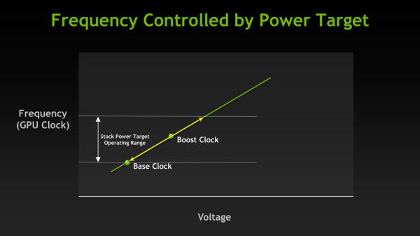
In a nutshell, GPU Boost is turbo for the GPU. With GPU Boost NVIDIA is able to increase the core clock of GTX beyond its 1006MHz base clock, and like turbo on CPUs this is based on the power load, the GPU temperature, and the overall quality of the GPU. Given the right workload the GTX 680 can boost by 100MHz or more, while under a heavy workload the GTX 680 may not move past 1006MHz.
With GPU Boost in play this adds a new wrinkle to performance of course, but ultimately there are 2 numbers to pay attention to. The first number is what NVIDIA calls the base clock: this is another name for the regular core clock, and it represents the minimum full load clock for GTX 680; when operating at its full 3D clocks, the GTX 680 will never drop below this number.
The second number is what NVIDIA calls the boost clock, and this one is far more nebulous, as it relates to the operation of GPU Boost itself. With GPU Boost NVIDIA does not have an explicit top clock; they’re letting chip quality play a significant role in GPU Boost. Because GPU Boost is based around power consumption and temperatures, higher quality GPUs that operate with lower power consumption can boost higher than lower quality GPUs with higher power consumption. In essence the quality of the chip determines its boost limit under normal circumstances.
Accordingly, the boost clock is intended to convey what kind of clockspeeds buyers can expect to see with the average GTX 680. Specifically, the boost clock is based on the average clockspeed of the average GTX 680 that NVIDIA has seen in their labs. This is what NVIDIA had to say about the boost clock in their reviewer’s guide:
The “Boost Clock” is the average clock frequency the GPU will run under load in many typical non-TDP apps that require less GPU power consumption. On average, the typical Boost Clock provided by GPU Boost in GeForce GTX 680 is 1058MHz, an improvement of just over 5%. The Boost Clock is a typical clock level achieved running a typical game in a typical environment
In other words, when the average GTX 680 is boosting it reaches 1058MHz on average.
Ultimately NVIDIA and their customers are going to go through some teething issues on this, and there’s no way around it. Although the idea of variable performance isn’t a new one – we already see this to some degree with CPU turbo – this is the first time we’ve seen something like this in the GPU space, and it’s going to take some time to get used to.
In any case while we can’t relate to you what the average GTX 680 does with GPU Boost, we can tell you about GPU Boost based on what we’ve seen with our review sample.
First and foremost, GPU Boost operates on the concept of steps, analogous to multipliers on a CPU. Our card has 9 steps, each 13MHz apart, ranging from 1006MHz to 1110MHz. And while it’s not clear whether every GTX 680 steps up in 13MHz increments, based on NVIDIA’s boost clock of 1058MHz this would appear to be the case, as that would be 4 steps over the base clock.
At each step our card uses a different voltage, listed in the table below. We should note that we’ve seen different voltages reported for the same step in some cases, so it’s not entirely clear what’s going on. In any case we’re listing the most common voltage we’ve recorded for each step.
| GeForce GTX 680 GPU Boost Step Table | |||
| Frequency | Voltage | ||
| 1110MHz | 1.175v | ||
| 1097MHz | 1.15v | ||
| 1084MHz | 1.137v | ||
| 1071MHz | 1.125v | ||
| 1058MHz | 1.125v | ||
| 1045MHz | 1.112v | ||
| 1032MHz | 1.100v | ||
| 1019MHz | 1.075v | ||
| 1006MHz | 1.062v | ||
As for deciding what clockspeed to step up to, GPU boost determines this based on power consumption and GPU temperature. NVIDIA has on-card sensors to measure power consumption at the rails leading into the GPU, and will only allow the video card to step up so long as it’s below the GPU Boost power target. This target isn’t published, but NVIDIA has told us that it’s 170W. Note that this is not the TDP of the card, which is 195W. Because NVIDIA doesn’t have a true throttling mechanism with Kepler, their TDP is higher than their boost target as heavy workloads can push power consumption well over 170W even at 1006MHz.
Meanwhile GPU temperatures also play an important role in GPU boost. Our sample could only hit the top step (1110MHz) if the GPU temperature was below 70C; as soon as the GPU reached 70C it would be brought down to the next highest step of 1097MHz. This means that the top step is effectively unsustainable on the stock GTX 680, as there are few if any applications that are both intensive enough to require high clockspeeds and light enough to not push GPU temperatures up.
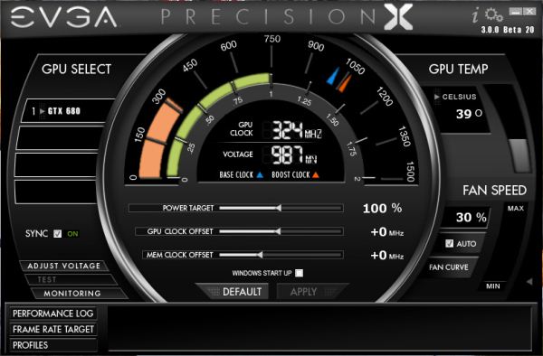
Finally, with the introduction of GPU Boost overclocking has been affected as well. Rather than directly controlling the core clock, overclocking is accomplished through the combined manipulation of the GPU Boost power target and the use of a GPU clock offset. Power target manipulation works almost exactly as you’d expect: you can lower and raise the GPU Boost power target by -30% to +32%, similar to how adjusting the PowerTune limit works on AMD cards. Increasing the power target allows the video card to pull more power, thereby allowing it to boost to higher steps than is normally possible (but no higher than the max step), while decreasing the power target keeps it from boosting at all.
The GPU offset meanwhile manipulates the steps themselves. By adjusting the GPU offset all of the GPU Boost steps are adjusted by roughly an equal amount, depending on what clocks the PLL driving the GPU can generate. E.G. a +100MHz offset clock would increase the 1st step to 1120MHz, etc up to the top step which would be increased to 1210MHz.
While each factor can be adjusted separately, it’s adjusting both factors together that truly unlock overclocking. Adjusting the GPU offset alone won’t achieve much if most workloads are limited by GPU Boost’s power target, and adjusting the power target alone won’t improve the performance of workloads that are already allowed to reach the highest step. By combining the two you can increase the GPU clock and at the same time increase the power target so that workloads are actually allowed to hit those new clocks.
On that note, overclocking utilities will be adding support for GPU Boost over the coming weeks. The first overclocking utility with support for GPU Boost is EVGA’s Precision X, the latest rendition of their Precision overclocking utility. NVIDIA supplied Precision X Beta 20 with our review samples, and as we understand it that will be made available shortly for GTX 680 buyers.
Finally, while we’ll go into full detail on overclocked performance in a bit, we wanted to quickly showcase the impact GPU Boost, both on regular performance and on overclocking. First up, we ran all of our benchmarks at 2560 with the power target for GPU boost set to -16%, which reduces the power target to roughly 142W. While GPU Boost cannot be disabled outright, this was enough to ensure that it almost never activated.
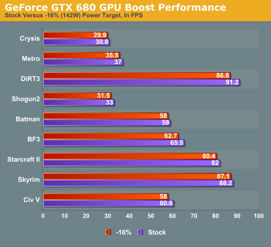
As is to be expected, the impact of GPU Boost varies depending on the game, but overall we found that enabling GPU boost on our card only improves performance by an average of 3%, and by no more than 5%. While this is effectively free performance, it also is a stark reminder that GPU Boost isn’t nearly as potent as turboing on a CPU – at least not quite yet. As there’s no real equivalent to the lightly threaded workload for GPUs, the need for a wide range of potential GPU Boost clocks is not nearly as great as the need for high turbo clocks on a CPU. Even a light GPU workload is relatively heavy when graphics itself is an embarrassingly parallel task.
Our other quick look is at overclocking. The following is what our performance looked like at 2560 with stock GPU Boost settings, a power target of +16% (195W), and a GPU offset of +100MHz.
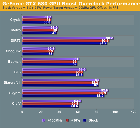
Overall raising the GPU offset is much more effective than raising the power target to improve performance, reflecting the fact that in our case most games were limited by the GPU Boost clock rather than the power target at least some of the time.
Meet the GeForce GTX 680
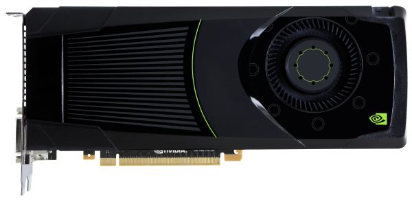
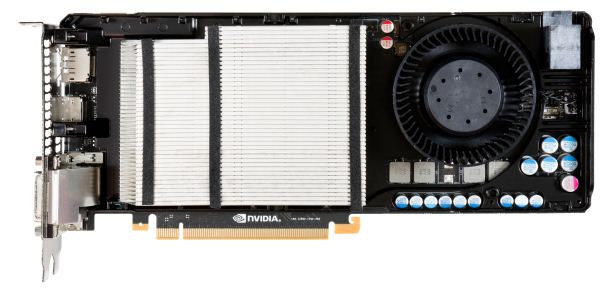
All things considered the design of the GeForce GTX 680 is not a radical departure from the GTX 580, but at the same time it also has some distinct differences owing to the fact that its TDP is some 50W lower than GTX 580.
Like the past GTX x80 cards, the basic design of the GTX 680 is that of a blower. A radial fan at the rear of the card sucks in air and pushes it towards the front of the card. Notably, due to a combination of card length and the fan position, the “wedge” around the fan has been done away with. NVIDIA tells us that this shouldn’t significantly impact the cooling of the card, particularly since it has a lower TDP in the first place, but when used in SLI it will remove some of the breathing room than the GTX 580 enjoyed.
Looking at the fan itself, compared to the GTX 580 the fan has been moved from the center of the card to the top of the card. This is due to NVIDIA’s port configuration, which uses a stacked DVI connector that consumes what would have normally been part of the exhaust vent on the GTX 580. We’ll get into the port configuration more in a minute, but for the moment the significance is that because the GTX 680 only has half a vent NVIDIA has moved the fan to match the vent, which is why the fan has been moved up.
On that note, the repositioning of the fan also had its own ramifications. Because the fan is now so close to the top and at the same time so close to the rear, NVIDIA went with a unique method of arranging the PCIe power sockets. Rather than having them side-by-side as we’ve seen on countless NVIDIA cards in the past, the sockets are stacked on each other in a staggered configuration. With the fan otherwise occupying the space that one of the sockets would take up, this configuration allowed NVIDIA to have two sockets without lengthening the card just to fit another socket. Overall this staggered design is not too difficult to work with, though with one socket facing the opposite way it might require some cable repositioning if you have a well maintained cable run.
Moving on, when we remove the shroud on the GTX 680 we see the fan, baseplate, and heatsink in full detail. NVIDIA is using an aluminum fin stacked heatsink, very similar to what we saw on the GTX 580. Underneath the heatsink NVIDIA is using a set of three heatpipes to transfer heat between the GPU and the heatsink. This is as opposed to the vapor chamber on the GTX 580, and while this setup doesn’t allow empirical testing, given the high efficiency of vapor chambers it’s likely that this isn’t quite as efficient, though to what degree we couldn’t say.
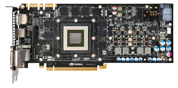
Finally, after removing the fan, baseplate, and heatsink, we can see the PCB in full detail. Unlike GF110 and GF114, GK104 is not capped with an IHS, allowing for the heatsink to directly come in contact with the GPU die. Meanwhile arranged around the GPU we can see the 8 2Gb GDDR5 RAM modules that give the GTX 680 its 2GB of RAM. These are Hynix R0C modules, which means they’re rated for 6GHz, the stock memory speed for the GTX 680. Overall the card measures 10” long with no overhang from the shroud, making it 0.5” shorter than the GTX 580.
Looking at the top of the card, as always we see the SLI connectors. Following in the footsteps of the GTX 580, the GTX 680 features 2 SLI connectors, allowing for up to 3-way SLI.
Meanwhile at the front of the card we see the I/O bracket. As we alluded to previously, the GTX 680 uses a stacked DVI design here; NVIDIA has done everything they can to keep the DVI ports at the very bottom of the card to avoid impeding airflow, but the upper DVI port still occupies roughly 40% of what would otherwise be the vent. Altogether the GTX 680 features 2 DL-DVI ports, a full size HDMI port, and a full size DisplayPort.
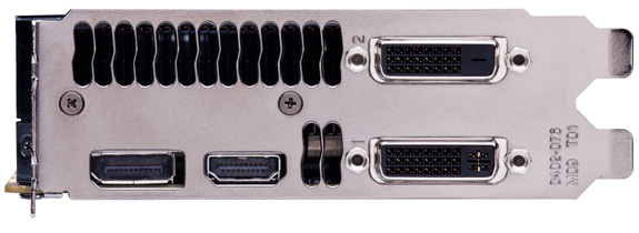
While NVIDIA has used DVI and HDMI ports for quite some time, this is the first time NVIDIA has included DIsplayPort on a reference design. Unfortunately we find that this ruffles our feathers a bit, although this isn’t strictly NVIDIA’s fault. As we’ve covered in the past, DisplayPort comes in both a full size and miniDP configuration – AMD in particular has used miniDP since the Radeon HD 6800 series in 2010. And while we’re happy to see DisplayPort finally make it into an NVIDIA reference design, the fact that it’s a full size DisplayPort is less than encouraging because at this point in time DisplayPort has largely been replaced by miniDP.
Ultimately the fault for this lies more with the VESA than NVIDIA, but it’s indicative of a larger problem in the DisplayPort community in that both full size DP and miniDP are equally valid and equally capable ports. While full size DisplayPort has the distinction of coming first, thanks in large part to Apple it has largely been displaced by miniDP as the most common variant on source devices. The problem with this is that both miniDP and DisplayPort are now in wide use; wide, redundant use.
At this point desktop computers and video cards coming with full size DisplayPorts is silly at best, and frustrating at worst. The laptop guys aren’t going to give up miniDP due to the space savings, and there’s no significantly good reason to use DisplayPort on desktops when miniDP offers the same functionality. We would rather see the PC industry standardize on miniDP across all source devices, and thereby eliminate any ambiguity with regards to what cables or adaptors are necessary. DisplayPort adoption has been slow enough – having 2 variants of the port on source devices only makes it more confusing for everyone.
Finally, while we’re on the subject of display connectivity we quickly took a look at how the idle clockspeeds of GTX 680 are impacted by the use of multiple displays. With 2 displays GTX 680 can utilize its full idle clocks, but only if both displays are connected via a TMDS type connection (DVI/HDMI) and run with identical timings. But if different timings are used or if one display is connected via DisplayPort, then the GTX 680 will shift to its low power 3D clocks. However if we expand that to 3 monitors and enable NVIDIA Surround, then the GTX 680 can operate at full idle regardless of whether DisplayPort is used or not.
The Test
For the GTX 680 launch, the press review driver is 300.99, while the launch driver is 301.10. This driver currently only works with the GTX 680, but NVIDIA will eventually be rolling out a version of the driver that includes support for older cards, which will bring with it official support for driver forced FXAA on Fermi cards. 300.99 is otherwise identical to the 290 series, and has no other changes or new features that we haven’t otherwise mentioned.
| CPU: | Intel Core i7-3960X @ 4.3GHz |
| Motherboard: | EVGA X79 SLI |
| Chipset Drivers: | Intel 9.2.3.1022 |
| Power Supply: | Antec True Power Quattro 1200 |
| Hard Disk: | Samsung 470 (256GB) |
| Memory: | G.Skill Ripjaws DDR3-1867 4 x 4GB (8-10-9-26) |
| Case: | Thermaltake Spedo Advance |
| Video Cards: |
AMD Radeon HD 7950 AMD Radeon HD 7870 AMD Radeon HD 7850 AMD Radeon HD 6990 AMD Radeon HD 6970 AMD Radeon HD 6950 AMD Radeon HD 5870 AMD Radeon HD 4870 AMD Radeon HD 3870 NVIDIA GeForce GTX 680 NVIDIA GeForce GTX 590 NVIDIA GeForce GTX 580 NVIDIA GeForce GTX 570 NVIDIA GeForce GTX 560 Ti NVIDIA GeForce GTX 285 NVIDIA GeForce 8800GT |
| Video Drivers: |
NVIDIA ForceWare 296.10 NVIDIA ForceWare 300.99 AMD Catalyst Beta 8.95.5 |
| OS: | Windows 7 Ultimate 64-bit |
Crysis: Warhead
Kicking things off as always is Crysis: Warhead. It’s no longer the toughest game in our benchmark suite, but it’s still a technically complex game that has proven to be a very consistent benchmark. Thus even four years since the release of the original Crysis, “but can it run Crysis?” is still an important question, and the answer continues to be “no.” While we’re closer than ever, full Enthusiast settings at a 60fps is still beyond the grasp of a single-GPU card.
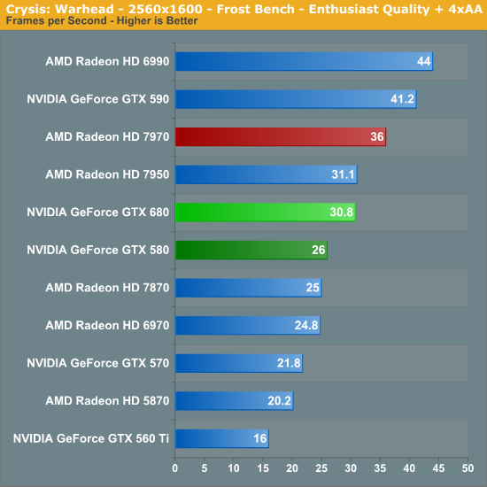
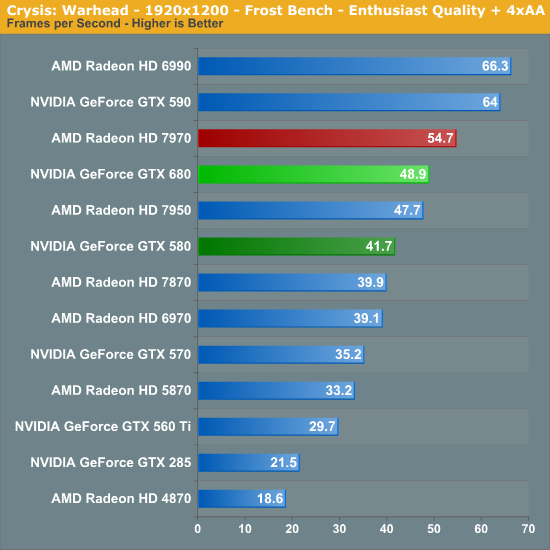
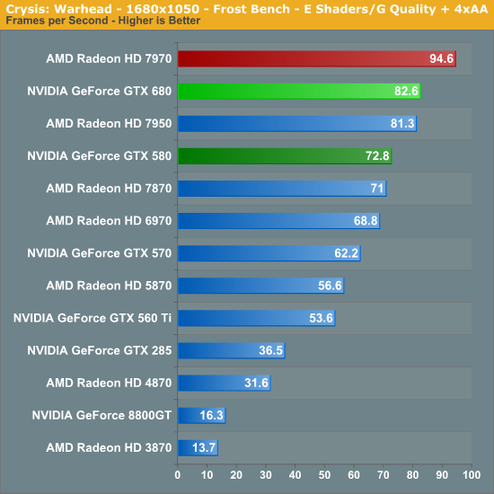
While Crysis was a strong game for the GTX 580, the same cannot be said of the GTX 680. NVIDIA is off to a very poor start here, with the Radeon HD 7970 easily outperforming the GTX 680, and even the 7950 is tied or nearly tied with the GTX 680 depending on the resolution. On the bright side the GTX 680 does manage to outperform the GTX 580, but only by a relatively meager 17%.
Given the large gap in theoretical performance between the GTX 680 and GTX 580, as it turns out we’ve run into one of the few scenarios where the GTX 680 doesn’t improve on the GTX 580: memory bandwidth. In our overclocking results we discovered that a core overclock had almost no impact on Crysis, whereas a memory overclock improved performance by 8%, almost exactly as much as the memory overclock itself. When it comes to the latest generation of cards it appears that Crysis loves memory bandwidth, and this is something the Radeon HD 7900 series has in spades but the GTX 680 does not. Thankfully for NVIDIA not every game is like Crysis.
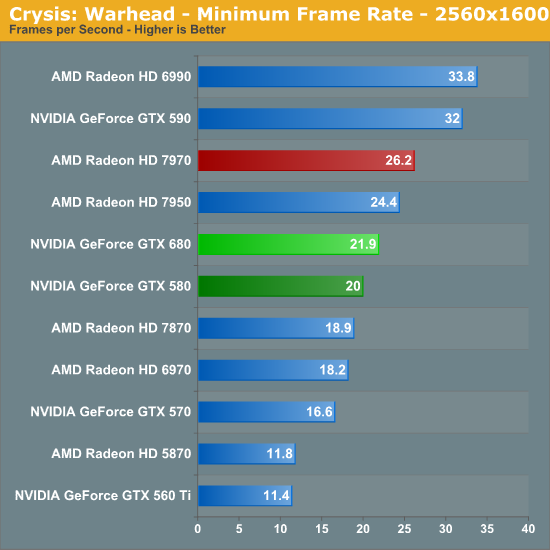
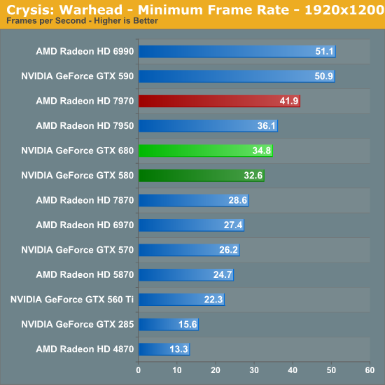
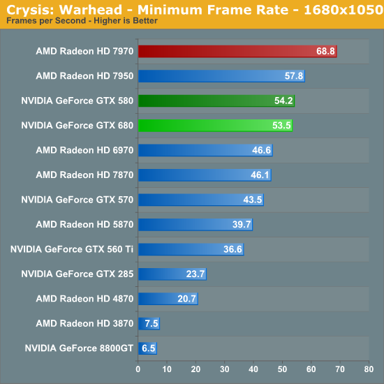
The minimum framerate situation is even worse for NVIDIA here, with the GTX 680 clearly falling behind the 7950, and improving on the GTX 580 by only 10%. At its worst Crysis is absolutely devouring memory bandwidth here, and that leaves the GTX 680 underprepared.
Metro 2033
Paired with Crysis as our second behemoth FPS is Metro: 2033. Metro gives up Crysis’ lush tropics and frozen wastelands for an underground experience, but even underground it can be quite brutal on GPUs, which is why it’s also our new benchmark of choice for looking at power/temperature/noise during a game. If its sequel due this year is anywhere near as GPU intensive then a single GPU may not be enough to run the game with every quality feature turned up.
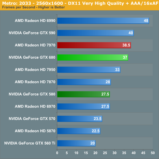
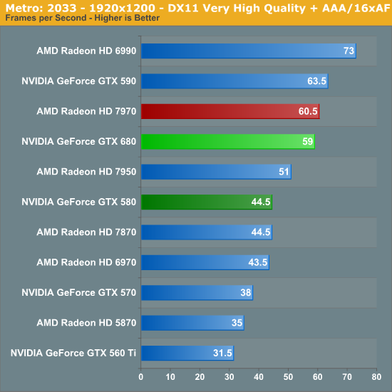
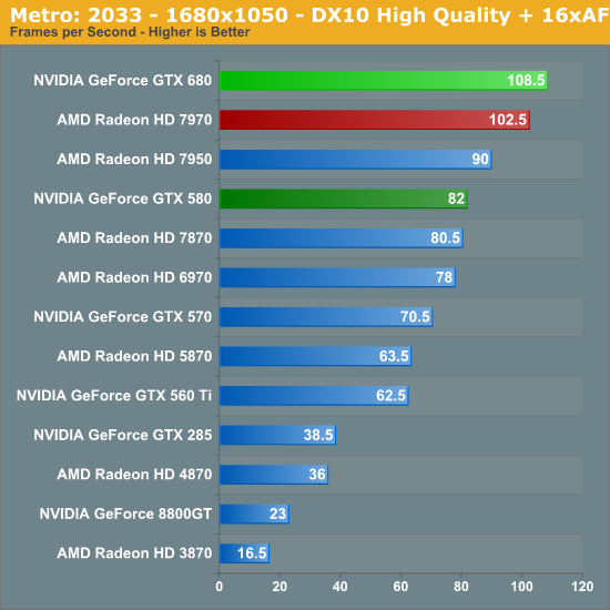
Thankfully for NVIDIA Metro is much, much better than Crysis for the GTX 680. The GTX 680 still trails the 7970 by a few percent at 2560, but it’s now clearly ahead of the 7950. Performance relative to the GTX 580 is far better, with the GTX 680 leading by 34%. In our experience Metro is very shader heavy, and this would appear to be confirmation of that as the GTX 680 has far greater shader resources than GTX 580.
What’s particularly interesting here though is that the GTX 680 has nearly caught up with the GTX 590. NVIDIA’s SLI scaling for Metro isn’t particularly fantastic, but it’s still quite a leap compared to the GTX 580. Consequently this is the first sign that the GTX 680 can compete with the GTX 590, which would be quite an accomplishment.
DiRT 3
For racing games our racer of choice continues to be DiRT, which is now in its 3rd iteration. Codemasters uses the same EGO engine between its DiRT, F1, and GRID series, so the performance of EGO has been relevant for a number of racing games over the years.
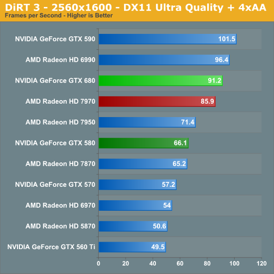
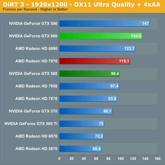
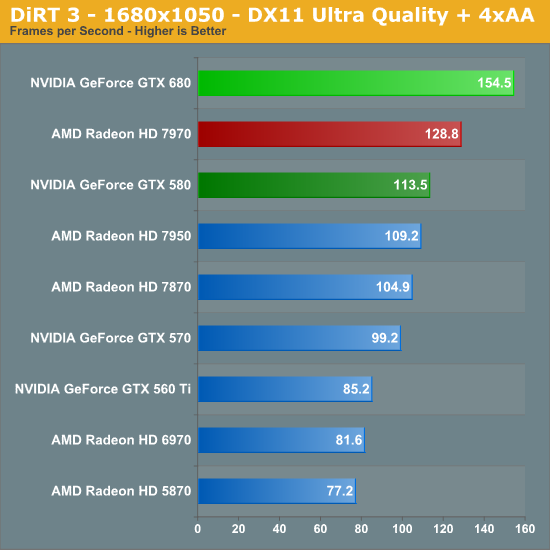
First it loses, then it ties, and then it starts to win.
After a very poor start in Crysis NVIDIA has finally taken a clear lead in a game. DiRT 3 has historically favored NVIDIA’s video cards so this isn’t wholly surprising, but it’s our first proof that the GTX 680 can beat the 7970, with the GTX 680 taking a respectable 6% lead at 2560. Interestingly enough the lead increases as we drop down in resolution, which is something we have also seen with past Radeon and GeForce cards. It looks like Fermi’s trait of dropping off in performance more rapidly with resolution than GCN has carried over to the GTX 680.
In any case, compared to the GTX 580 this is another good showing for the GTX 680. The 680’s lead on the 580 is a rather consistent 36-38%.
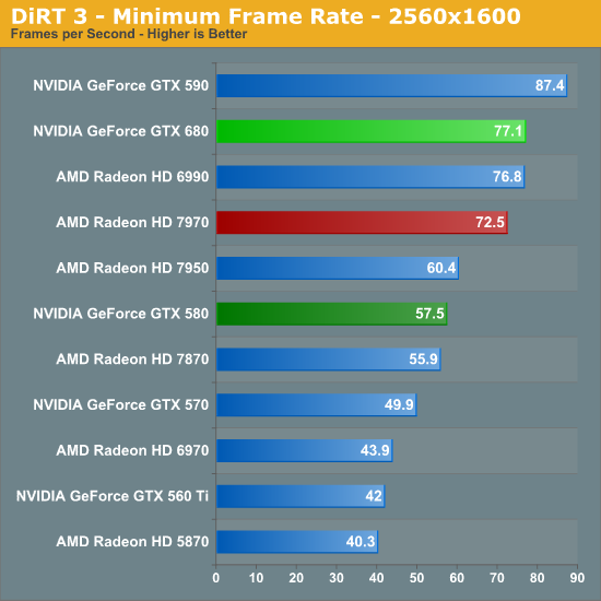
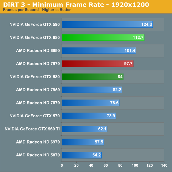
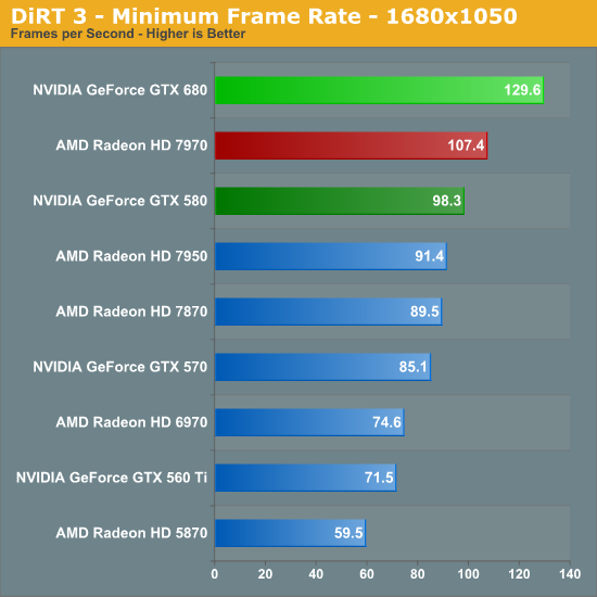
The minimum framerates reflect what we’ve seen with the averages; the GTX 680 has a slight lead on the 7970 at 2560, while it beats the GTX 580 by over 30%.
Total War: Shogun 2
Total War: Shogun 2 is the latest installment of the long-running Total War series of turn based strategy games, and alongside Civilization V is notable for just how many units it can put on a screen at once. As it also turns out, it’s the single most punishing game in our benchmark suite (on higher end hardware at least).
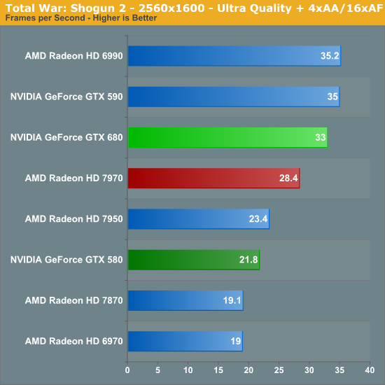
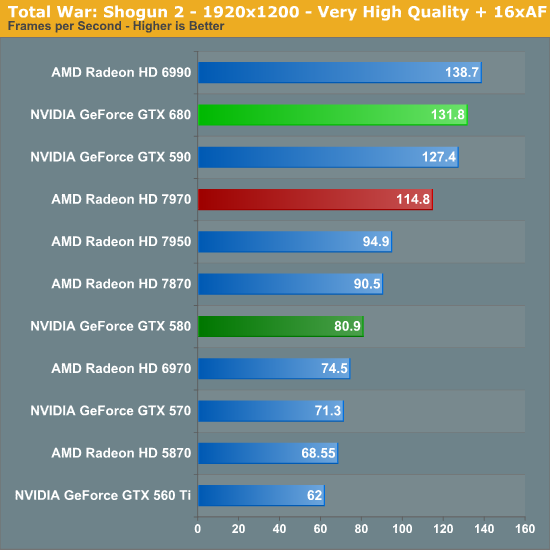
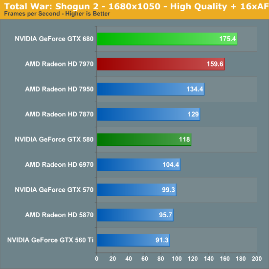
With Shogun 2 the GTX 680 sees its first decisive win at last. At the all-punishing resolution of 2560 the GTX 680 not only becomes the first single-GPU card to crack 30fps, but it takes a 16% lead over the 7970 here. Even at a more practical resolution and setting of 1920 the GTX 680 still leads by 15%. Meanwhile the GTX 580 fares even worse here, with the GTX 680 leading by 51% at 2560 and a whopping 63% at 1920. Even the GTX 590 can only barely beat the GTX 680 at 2560, only to lose at 1920.
At this point we’re not sure what it is about the GTX 680 that improves on the GTX 580 by so much. Shogun 2 does use a lot of VRAM, and while the greater amount of VRAM on the GTX 680 alone wouldn’t seem to explain this, the fact that most of that memory is consumed by textures just might. We may be seeing the benefit of the much greater number of texture units GTX 680 has.
Batman: Arkham City
Batman: Arkham City is loosely based on Unreal Engine 3, while the DirectX 11 functionality was apparently developed in-house. With the addition of these features Batman is far more a GPU demanding game than its predecessor was, particularly with tessellation cranked up to high.
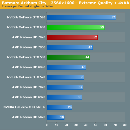
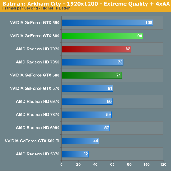
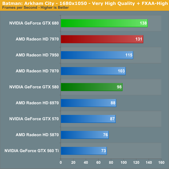
Once again the GTX 680 takes a respectable lead over the 7970, this time beating AMD’s top card by 13% at 2560, and coming very close to cracking 60fps here. The performance gains over the GTX 580 are also solid, with the GTX 680 leading by 34% or better.
Portal 2
Portal 2 continues the long and proud tradition of Valve’s in-house Source engine. While Source continues to be a DX9 engine, Valve has continued to upgrade it over the years to improve its quality, and combined with their choice of style you’d have a hard time telling it’s over 7 years old at this point. Consequently Portal 2’s performance does get rather high on high-end cards, but we have ways of fixing that…
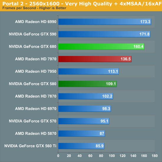
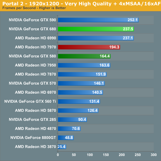
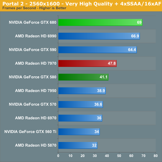
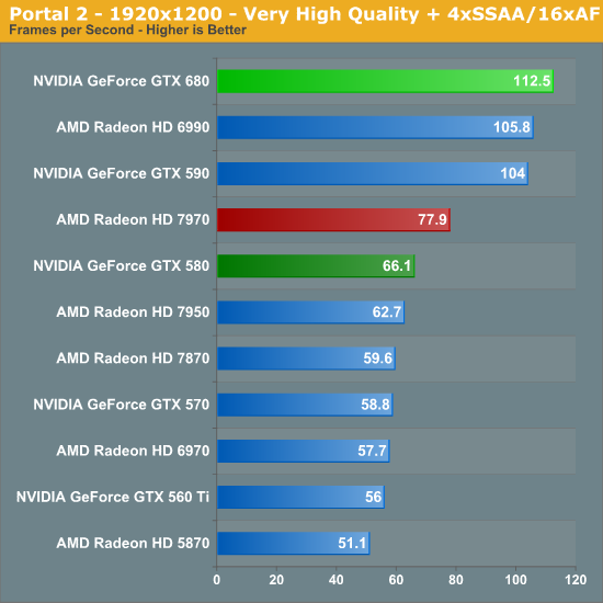
Portal 2 ends up being the strongest lead yet for the GTX 680, with the GTX 680 taking a 17% lead at 2560. What’s especially interesting though is performance in the bonus round with SSAA enabled – the GTX 680 takes a wholly unexpected and completely stunning 44% lead over the 7970. In fact it beats out everything here, including the GTX 590 and Radeon HD 6990. Meanwhile the lead over the GTX 580 is even more amazing, with the GTX 680 leading by 67% at these settings.
As it stands the GTX 680 is the first single-GPU card to do better than 60fps, and it does so in a landslide. All things considered, for a lack of memory bandwidth and ROP changes compared to Fermi GTX 680 does extremely well here.
Battlefield 3
Its popularity aside, Battlefield 3 may be the most interesting game in our benchmark suite for a single reason: it’s the first AAA DX10+ game. It’s been 5 years since the launch of the first DX10 GPUs, and 3 whole process node shrinks later we’re finally to the point where games are using DX10’s functionality as a baseline rather than an addition. Not surprisingly BF3 is one of the best looking games in our suite, but as with past Battlefield games that beauty comes with a high performance cost

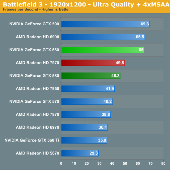
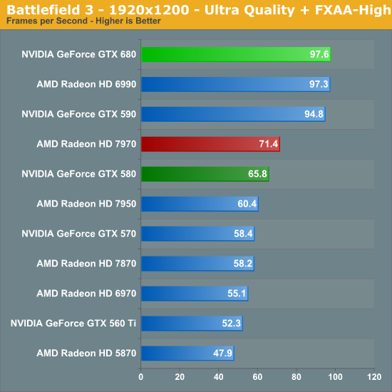
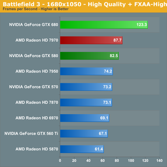
NVIDIA’s cards have always done well at Battlefield 3, which puts the Radeon HD 7900 series in a bad position from the beginning. Short of the GTX 680’s massive lead in the Portal 2 bonus round, this is the single biggest victory for the GTX 680 over the 7970, beating AMD’s best by 28% at 2560, and by continually higher amounts at lower resolutions. Based on our experience with BF3 I’d hesitate to call the 680 fully fluid at 2560 as large firefights can significantly tear into performance relative to Thunder Run, but if it’s not fully fluid then it’s going to be very, very close.
What’s also interesting here is that once again the GTX 680 is doing very well compared to the dual-GPU cards. The GTX 590 and 6990 never pull away from the GTX 680, and at 1920 with FXAA the GTX 680 finally squeaks by and takes the top of the chart. Performance relative to the GTX 580 is also once again good for that matter, with the GTX 680 beating its predecessor by 48% at almost every resolution.
Starcraft II
Our next game is Starcraft II, Blizzard’s 2010 RTS megahit. Much like Portal 2 it’s a DX9 game designed to run on a wide range of hardware so performance is quite peppy with most high-end cards, but it can still challenge a GPU when it needs to.
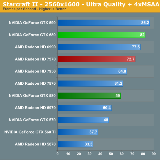
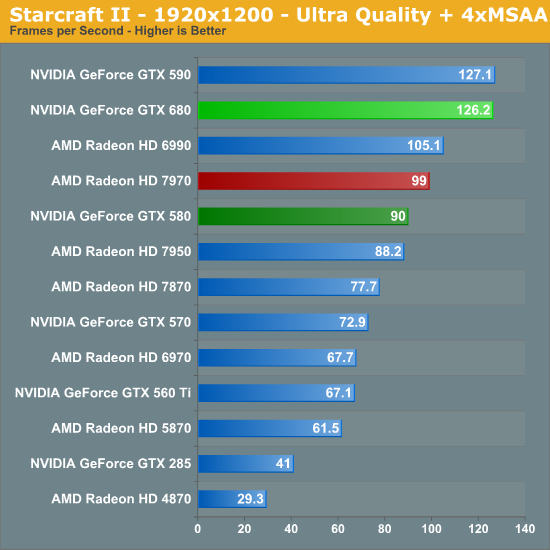
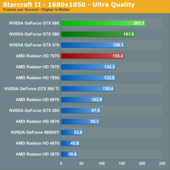
While AMD tends to suffer in Starcraft II at lower resolutions, at 2560 we tend to get a good brawl and the GTX 680 doesn’t disappoint. Here it leads the 7970 by 13% and leads the GTX 580 by 39%.
The Elder Scrolls V: Skyrim
Prior to the launch of our new benchmark suite, we wanted to include The Elder Scrolls V: Skyrim, which is easily the most popular RPG of 2011. However as any Skyrim player can tell you, Skyrim’s performance is CPU-bound to a ridiculous degree. With the release of the 1.4 patch and the high resolution texture pack this has finally been relieved to the point where GPUs once again matter, particularly when we’re working with high resolutions and less than high-end GPUs. As such, we're now including it in our test suite.
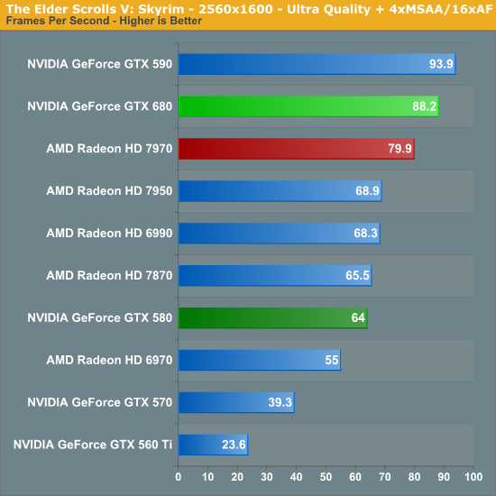
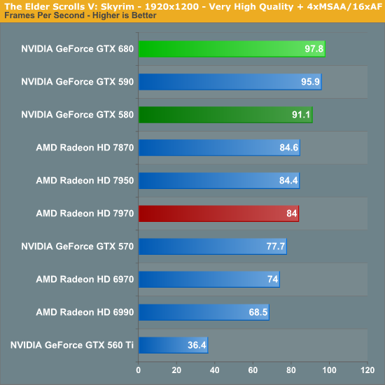
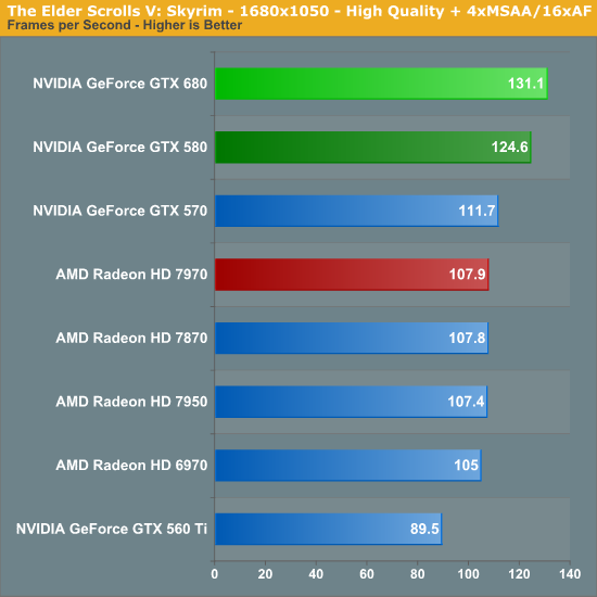
Skyrim presents us with an interesting scenario. At anything less than 2560 we’re CPU limited well before we’re GPU limited, and yet even though we’re CPU limited NVIDIA manages to take a clear lead while the 680 still finds room to push to the top. For whatever the reason NVIDIA would appear to have significantly less driver overhead here, or at the very least a CPU limited Skyrim interacts with NVIDIA’s drivers better than it does AMD’s.
In any case 2560 does move away from being CPU limited, but it’s not entirely clear whether the difference we’re seeing here is solely due to GPU performance, or if we’re still CPU limited in some fashion. Regardless of the reason the GTX 680 has a 10% lead on the 7970 here.
Civilization V
Our final game, Civilization 5, gives us an interesting look at things that other RTSes cannot match, with a much weaker focus on shading in the game world, and a much greater focus on creating the geometry needed to bring such a world to life. In doing so it uses a slew of DirectX 11 technologies, including tessellation for said geometry, driver command lists for reducing CPU overhead, and compute shaders for on-the-fly texture decompression.
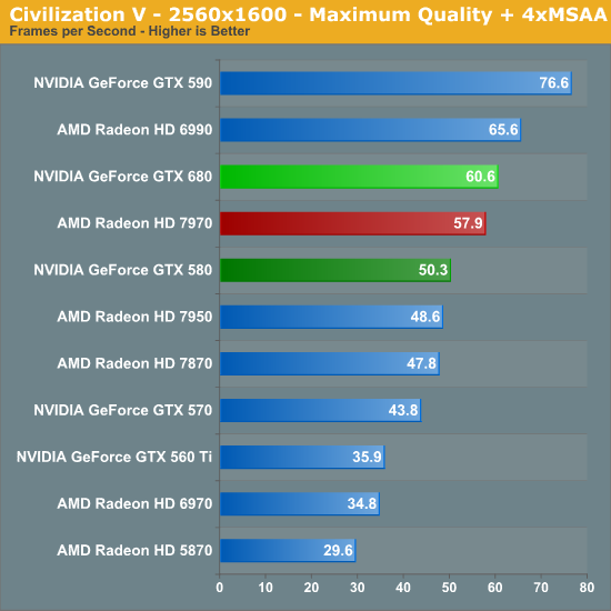
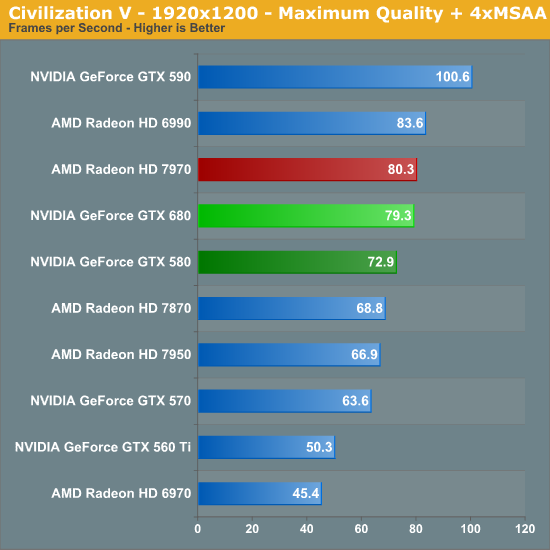
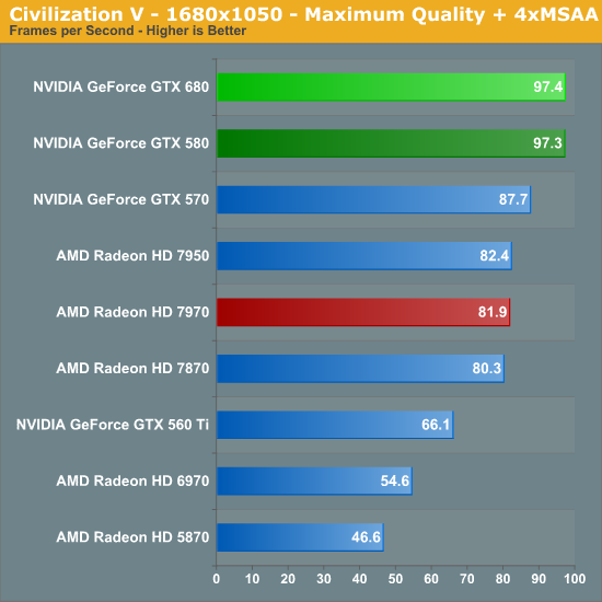
Remember when NVIDIA used to sweep AMD in Civ V? Times have certainly changed in the last year, that’s for sure. It only seems appropriate that we’re ending on what’s largely a tie. At 2560 the GTX 680 does have a 4% lead over the 7970, however the 7970 reclaims it’s lead at the last possible moment at 1920. At this point we’ve seen the full spectrum of results, from the GTX 680 losing badly to winning handily, and everything in between.
On a final note, it’s interesting to see that the GTX 680 really only manages to improve on the GTX 580’s performance at 2560. At 1920 the lead is only 8%, and at 1680 we’re just CPU limited. Haswell can’t get here soon enough.
Compute: What You Leave Behind?
As always our final set of benchmarks is a look at compute performance. As we mentioned in our discussion on the Kepler architecture, GK104’s improvements seem to be compute neutral at best, and harmful to compute performance at worst. NVIDIA has made it clear that they are focusing first and foremost on gaming performance with GTX 680, and in the process are deemphasizing compute performance. Why? Let’s take a look.
Our first compute benchmark comes from Civilization V, which uses DirectCompute to decompress textures on the fly. Civ V includes a sub-benchmark that exclusively tests the speed of their texture decompression algorithm by repeatedly decompressing the textures required for one of the game’s leader scenes. Note that this is a DX11 DirectCompute benchmark.
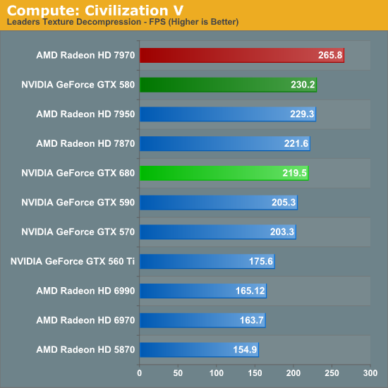
Remember when NVIDIA used to sweep AMD in Civ V Compute? Times have certainly changed. AMD’s shift to GCN has rocketed them to the top of our Civ V Compute benchmark, meanwhile the reality is that in what’s probably the most realistic DirectCompute benchmark we have has the GTX 680 losing to the GTX 580, never mind the 7970. It’s not by much, mind you, but in this case the GTX 680 for all of its functional units and its core clock advantage doesn’t have the compute performance to stand toe-to-toe with the GTX 580.
At first glance our initial assumptions would appear to be right: Kepler’s scheduler changes have weakened its compute performance relative to Fermi.
Our next benchmark is SmallLuxGPU, the GPU ray tracing branch of the open source LuxRender renderer. We’re now using a development build from the version 2.0 branch, and we’ve moved on to a more complex scene that hopefully will provide a greater challenge to our GPUs.
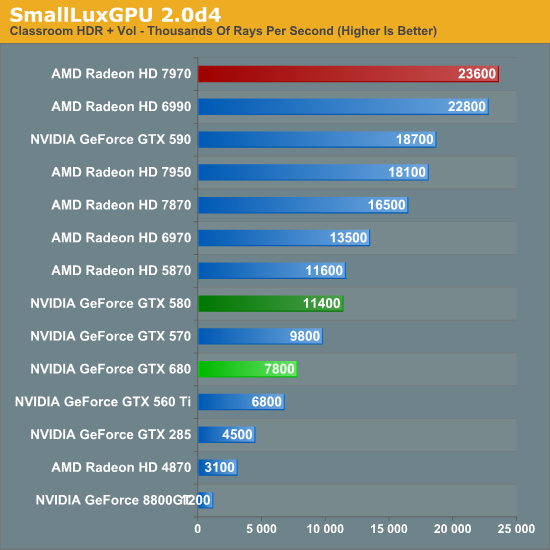
CivV was bad; SmallLuxGPU is worse. At this point the GTX 680 can’t even compete with the GTX 570, let alone anything Radeon. In fact the GTX 680 has more in common with the GTX 560 Ti than it does anything else.
On that note, since we weren’t going to significantly change our benchmark suite for the GTX 680 launch, NVIDIA had a solid hunch that we were going to use SmallLuxGPU in our tests, and spoke specifically of it. Apparently NVIDIA has put absolutely no time into optimizing their now all-important Kepler compiler for SmallLuxGPU, choosing to focus on games instead. While that doesn’t make it clear how much of GTX 680’s performance is due to the compiler versus a general loss in compute performance, it does offer at least a slim hope that NVIDIA can improve their compute performance.
For our next benchmark we’re looking at AESEncryptDecrypt, an OpenCL AES encryption routine that AES encrypts/decrypts an 8K x 8K pixel square image file. The results of this benchmark are the average time to encrypt the image over a number of iterations of the AES cypher.
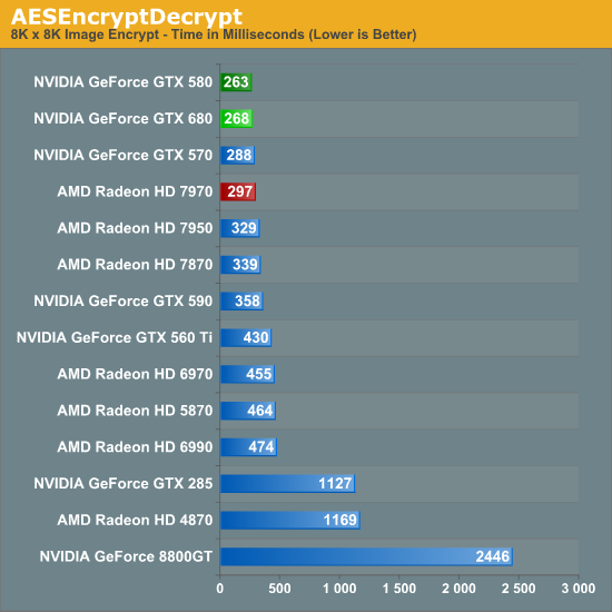
Starting with our AES encryption benchmark NVIDIA begins a recovery. GTX 680 is still technically slower than GTX 580, but only marginally so. If nothing else it maintains NVIDIA’s general lead in this benchmark, and is the first sign that GTX 680’s compute performance isn’t all bad.
For our fourth compute benchmark we wanted to reach out and grab something for CUDA, given the popularity of NVIDIA’s proprietary API. Unfortunately we were largely met with failure, for similar reasons as we were when the Radeon HD 7970 launched. Just as many OpenCL programs were hand optimized and didn’t know what to do with the Southern Islands architecture, many CUDA applications didn’t know what to do with GK104 and its Compute Capability 3.0 feature set.
To be clear, NVIDIA’s “core” CUDA functionality remains intact; PhysX, video transcoding, etc all work. But 3rd party applications are a much bigger issue. Among the CUDA programs that failed were NVIDIA’s own Design Garage (a GTX 480 showcase package), AccelerEyes’ GBENCH MatLab benchmark, and the latest Folding@Home client. Since our goal here is to stick to consumer/prosumer applications in reflection of the fact that the GTX 680 is a consumer card, we did somewhat limit ourselves by ruling out a number of professional CUDA applications, but there’s no telling that compatibility there would fare any better.
We ultimately started looking at Distributed Computing applications and settled on PrimeGrid, whose CUDA accelerated GENEFER client worked with GTX 680. Interestingly enough it primarily uses double precision math – whether this is a good thing or not though is up to the reader given the GTX 680’s anemic double precision performance.
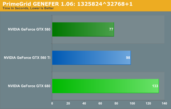
Because it’s based around double precision math the GTX 680 does rather poorly here, but the surprising bit is that it did so to a larger degree than we’d expect. The GTX 680’s FP64 performance is 1/24th its FP32 performance, compared to 1/8th on GTX 580 and 1/12th on GTX 560 Ti. Still, our expectation would be that performance would at least hold constant relative to the GTX 560 Ti, given that the GTX 680 has more than double the compute performance to offset the larger FP64 gap.
Instead we found that the GTX 680 takes 35% longer, when on paper it should be 20% faster than the GTX 560 Ti (largely due to the difference in the core clock). This makes for yet another test where the GTX 680 can’t keep up with the GTX 500 series, be it due to the change in the scheduler, or perhaps the greater pressure on the still-64KB L1 cache. Regardless of the reason, it is becoming increasingly evident that NVIDIA has sacrificed compute performance to reach their efficiency targets for GK104, which is an interesting shift from a company that was so gung-ho about compute performance, and a slightly concerning sign that NVIDIA may have lost faith in the GPU Computing market for consumer applications.
Finally, our last benchmark is once again looking at compute shader performance, this time through the Fluid simulation sample in the DirectX SDK. This program simulates the motion and interactions of a 16k particle fluid using a compute shader, with a choice of several different algorithms. In this case we’re using an (O)n^2 nearest neighbor method that is optimized by using shared memory to cache data.
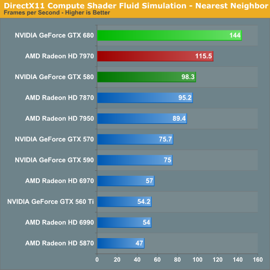
Redemption at last? In our final compute benchmark the GTX 680 finally shows that it can still succeed in some compute scenarios, taking a rather impressive lead over both the 7970 and the GTX 580. At this point it’s not particularly clear why the GTX 680 does so well here and only here, but the fact that this is a compute shader program as opposed to an OpenCL program may have something to do with it. NVIDIA needs solid compute shader performance for the games that use it; OpenCL and even CUDA performance however can take a backseat.
Theoreticals
As with any new architecture, we want to take a few moments to look at theoretical performance. These numbers shouldn’t be taken too seriously for cross-vendor comparison, but these numbers often tell us more about interesting architectural improvements that occur from one generation to the next.
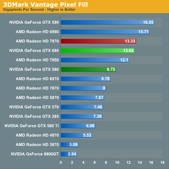
Our first theoretical test is perhaps the most perplexing: 3DMark Vantage’s pixel fill test. Typically this test is memory bandwidth bound as the nature of the test has the ROPs pushing as many pixels as possible with as little overhead as possible, which in turn shifts the bottleneck to a mix of ROP performance and the memory bandwidth needed to feed those ROPs.
Compared to the GTX 580, the GTX 680 has almost exactly the same amount of memory bandwidth (192GB/sec) and only 86% of the theoretical ROP performance (37Gpix vs. 32Gpix). In short, it shouldn’t outperform the GTX 580 here, and yet it outperforms the 580 by 33%.
Why does it do this? That’s the hard thing to answer. As we mentioned in our look at GK104’s architecture, NVIDIA did make some minor incremental improvements to their ROPs coming from GF114, such as slightly improved compression and improved polygon merging. One of those may very well be the contributing factor, particularly the compression improvements since this is a typically memory bandwidth bottlenecked test. Alternatively, it’s interesting to note that the difference between the two video cards is almost identical to the difference in the core clock. GTX 560 Ti’s results tend to blow a hole in this theory, but it bears consideration.
In any case, it’s an interesting turn of events and hopefully one that isn’t simply an edge case. As we’ve seen in our benchmarks GTX 680 has strong performance – even if its lead compared to the 7970 diminishes with resolution – but compared to the GTX 580 in particular it needs strong ROP performance across all games in order to deliver good performance at high resolutions and anti-aliasing.
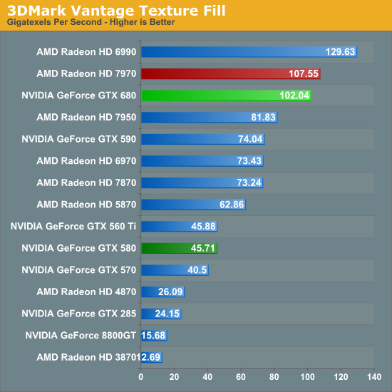
Our second theoretical test is 3DMark Vantage’s texture fill test, which to no surprise has the GTX 680 handily clobbering all prior NVIDIA cards. NVIDIA’s inclusion of 128 texture units on GK104 versus 64 on their previous generation GPUs gives the GTX 680 far better texturing performance. The 30%+ core clock difference only serves to further widen the gap.
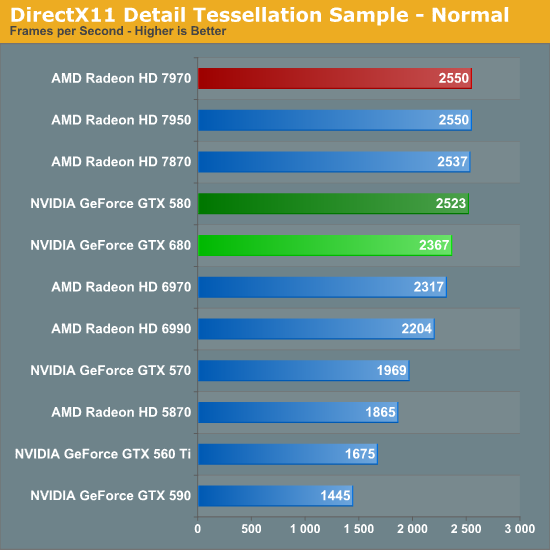
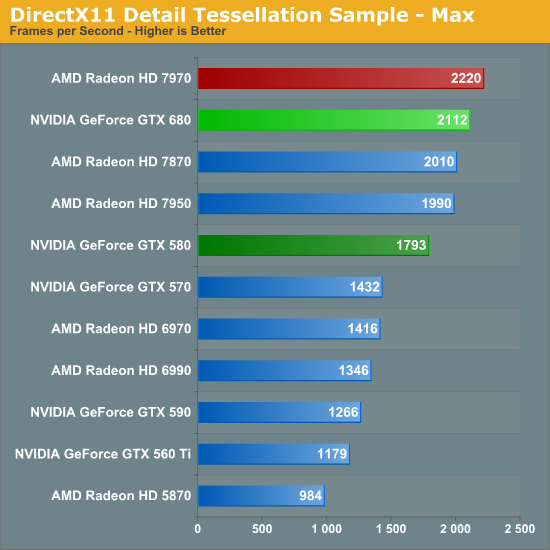
Our third theoretical test is the set of settings we use with Microsoft’s Detail Tessellation sample program out of the DX11 SDK. Overall while NVIDIA didn’t make any significant changes to their tessellation hardware (peak triangle rate is still 4/cycle), they have been working on further improving performance at absurdly high tessellation factors. You can see some of this in action at the max factor setting, but even then we’re running into a general performance wall since the Detail Tessellation program can’t go to the absolute highest tessellation factors NVIDIA’s hardware supports.
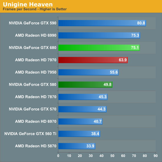
Our final theoretical test is Unigine Heaven 2.5, a benchmark that straddles the line between a synthetic benchmark and a real-world benchmark as the engine is licensed but no notable DX11 games have been produced using it yet. In any case the Heaven benchmark is notable for its heavy use of tessellation, which means it’s largely a proxy test for tessellation performance. Here we can see the GTX 680 shoot well ahead of the GTX 580 – by more than we saw in the DX11 Detail Tessellation sample – but at the same time there’s a lot more going on in Heaven than just tessellation.
Honestly at this point in time I’m not sure just how much more tessellation performance is going to matter. Until DX11 is the baseline API for games, tessellation is still an add-on feature, which means it’s being used to add fine detail to specific models rather than being used on everything in a game world. This demands good tessellation at high factors but at the same time it’s subject to diminishing returns on the improvement to image quality as triangles reach single pixel sizes and smaller. To that end I’m still waiting to see the day where we see tessellation scale similarly to textures – that is by using full MIP chaining of displacement maps – at which point we can evaluate tessellation performance similar to texture performance when it comes to both measuring the performance hit and evaluating the difference in image quality.
Power, Temperature, & Noise
As always, we’re wrapping up our look at a new video card’s stock performance with a look at power, temperature, and noise. With new process nodes being the lifeblood of the GPU industry, each new process gives GPU manufacturers a chance to move their product along a continuum; do they take advantage of a power consumption reduction for the same performance level, a performance increase for the same power consumption, or something in between? For NVIDIA the answer is a bit of “all of the above”, as while the GK104 based GTX 680 is more a direct successor of the GF114 based GTX 560 Ti in terms of how the GPU was built, NVIDIA has increased their power consumption while at the same time decreasing their die size relative to GF114.
| GeForce GTX 680 Voltages | ||||
| Ref GTX 680 Base Load | Ref GTX 680 Boost Load | Ref GTX 680 Idle | ||
| 1.062v | 1.175v | 0.987v | ||
As we noted in our look at GPU Boost, the operating voltage of the GTX 680 depends on the quality of the GPU and the clockspeed it runs at. The higher the clockspeed, the higher the operating voltage, starting from a typical voltage of 1.062v at the base clockspeed of 1006MHz, up to 1.175v at the peak clockspeed of our sample of 1110MHz. Idle voltages are far most consistent however, with the GTX 680 always dropping to 0.987v at idle.
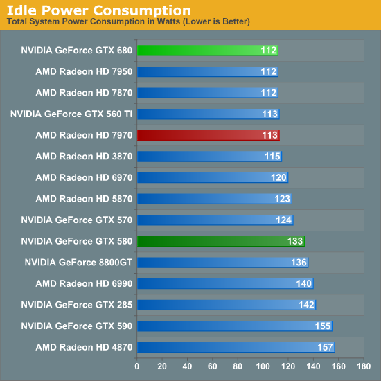
Speaking of idle, let’s start there. NVIDIA idle power consumption hasn’t significantly changed relative to GTX 560 Ti – not to say that NVIDIA hasn’t been working on this factor, but the low-hanging fruit has long been plucked. At 112W at the wall the GTX 680 is actually tied for the lowest power consumption among contemporary cards past and present, but with an estimated 15W idle TDP it’s not significantly different from any of those cards.
One interesting point though is that because GK104 is a GF114 derivative rather than a GF110 derivative, the GTX 680 does much better here compared to the GTX 580. We’re saving over 20W at the wall thanks to fewer RAM chips, less power regulation circuitry, and like most other things relating to GTX 680, a general increase in efficiency.
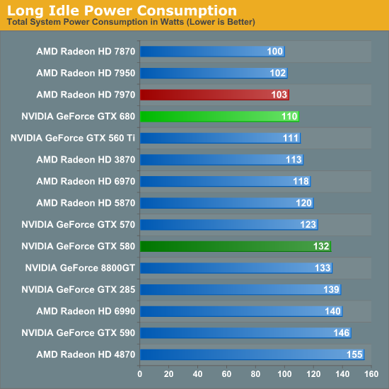
One thing NVIDIA specifically hasn’t touched though is the so-called “long idle” state where the system is powered up but the monitor is blank. GTX 680 shaves off a watt here versus GTX 560 Ti and 22W versus GTX 580, but without any special technology to further step down, they can’t match AMD and their ZeroCore Power technology.
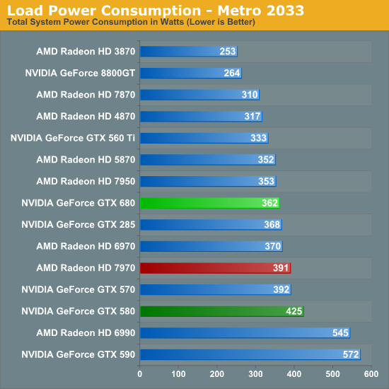
Shifting into load power consumption, our first measurement is from running our Metro 2033 benchmark. The results are roughly where we’d expect them, with the GTX 680 drawing more power than the GTX 560 Ti, but less power than the Radeon HD 7970, and compared to the GTX 580 significantly less power. Things are much closer compared to the 7950 however thanks to its similar 200W PowerTune limit, with the GTX 680 drawing only 9W more at the wall.
Because the performance of the video card here impacts the CPU load by requiring more frames to be prepared, power consumption does go up slightly with performance increases, which means some of the power consumption growth we’re seeing here relative to the GTX 560 Ti is a result of that performance gap, but measuring from the wall doesn’t let us fully separate it. NVIDIA’s power target GPU Boost on Metro 2033 is 170W, the same as the GTX 560 Ti’s TDP, but in all likelihood power consumption has jumped up at least 10W, while power consumption compared to the 7950 is probably a wash.
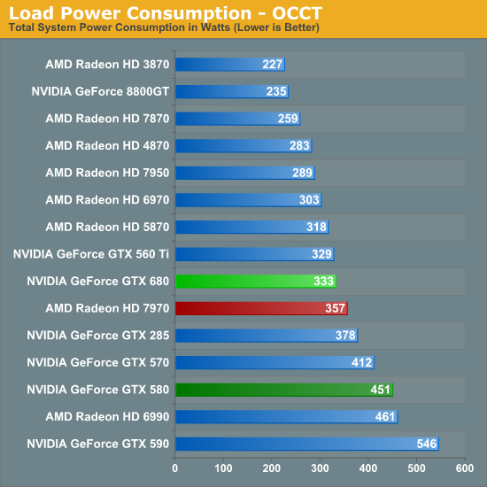
Our other power measurement is our pathological case with OCCT. In this case NVIDIA’s lack of a true throttling system continues to be to their disadvantage, as while AMD’s cards can cap their power consumption NVIDIA’s cards must keep going. In spite of this power consumption relative to the 7970 is still lower by 25W, but it blows past the 7950 by 44W. On the NVIDIA side of things though we can see just how much a smaller die and 28nm improve on matters compared to the GTX 580 – the 118W difference is nothing short of staggering. NVIDIA’s big GPUs can capture the performance crown, but they come with a high power cost, which makes taking the crown with the much smaller GK104 all the more important for NVIDIA.
On that note, it’s interesting to see that while power consumption runs high compared to AMD’s cards, compared to the GTX 560 Ti, power consumption has only ticked up by 4W. This reflects the fact that the GTX 680 is the successor to the GTX 560 Ti’s design, which means both cards have similar TDPs, though we would have actually expected the gap between the two to be wider. So in the worst case scenario NVIDA is exceeding our expectations.
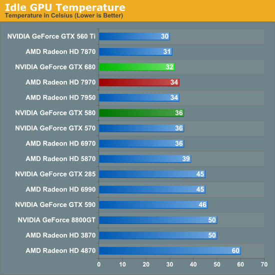
Moving past power consumption we have our look at temperatures, one of the two physical attributes that’s a derivative of power consumption. Idle temperatures aren’t too hard to do well at so long as your idle power consumption is solid and this is indeed the case for the GTX 680. The use of a blower means that NVIDIA can’t match the raw efficiency of the GTX 560 Ti, but they actually manage to edge out the Radeon HD 7900 series here. More to the point this continues what has been a long trend with regards to reducing idle temperatures; since the 8800GT the idle temperatures of NVIDIA’s top GPUs have dropped from a toasty 50C to 32C.
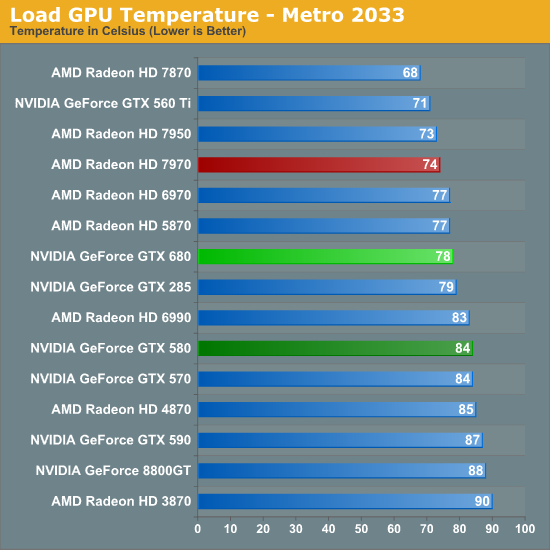
As for load temperatures, we’re once more in a familiar situation regarding NVIDIA and AMD design strategies. AMD’s aggressive cooling strategy keeps their 7900 cards in the mid-to-low 70s, while NVIDIA favors slightly higher temperatures for what we’ll see translates into less noise. At 78C under Metro NVIDIA is not repeating the common 80C+ temperatures the GTX 570 and GTX 580 reach, which is a reflection of the smaller GPU and smaller manufacturing process. NVIDIA’s max operating temperature for the GTX is 98C, so we have a good 20C to play with when it comes to overclocking.
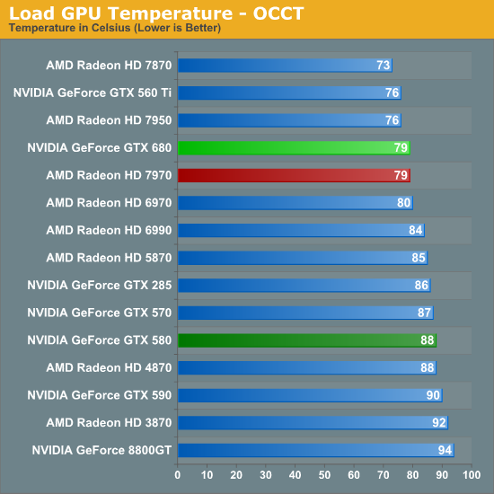
Switching over to OCCT, we suddenly find ourselves in an interesting situation when NVIDIA and AMD become relatively equalized. At 79C both the 7970 and GTX 680 are running at the same temperature, an unexpected situation given the latter’s lack of a throttling mechanism for OCCT. Once again it also drives a large gap between the GTX 680 and GTX 580, having reduced temperatures by 9C. And at the same time temperatures are up only 3C compared to the GTX 560 Ti, even with its lower power consumption and open air cooler. However if and when Big Kepler does come, I would expect GTX 580-like temperatures to return.
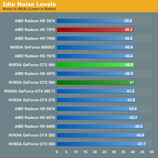
Last but not least we have our look at noise, which is typically the most important of the 3 physical attributes of a video card. Like idle temps, idle noise is largely a solved problem, which is why all of our results cluster around 40dB. The GTX 680 is 0.5dB quieter than the GTX 580 and 0.3dB louder than the 7970, but at this range the difference is nearly academic as noise from other system components is the biggest contributing factor.
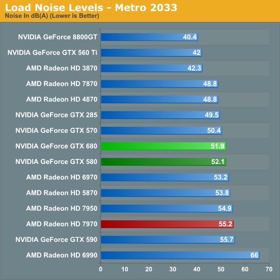
Now how does the GTX 680 fare in load noise? The answer depends on what you want to compare it to. Compared to the GTX 580, the GTX 680 is practically tied – no better and no worse – which reflects NVIDIA’s continued use of a conservative cooling strategy that favors noise over temperatures. At the same time, compared to the GTX 560 Ti this is a massive increase in noise, with just shy of a 10dB jump. The difference comes down to a few things, the most important of which is that the GTX 680 has a closed blower instead of the GTX 560 Ti’s unusually impressive open air cooler. At the same time as we’ve seen power consumption is up versus the GTX 560 Ti, so maintaining 42dB wouldn’t have been very practical even with another open air cooler.
Finally we have the Radeon comparison, where NVIDIA does quite well. AMD’s aggressive cooling strategy combined with the higher power consumption of the 7970 means that the 7970 is on the wrong side of the GTX 680 here, with the GTX 680 generating 3.3dB less noise. So while NVIDIA failed to significantly improve on the GTX 580 they did beat out AMD, which is going to be the more important difference for most buyers. All things considered I’m wondering if NVIDIA still couldn’t have done better here, but I think the limiting factor here is that NVIDIA doesn’t have a whole ventilation slot to work with.
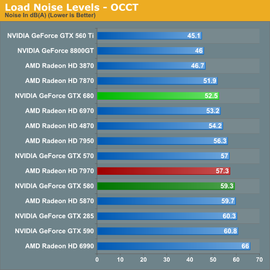
Last, but not least, we have our look at OCCT noise. Even with a lack of throttling, the smaller range between NVIDIA’s typical and max power consumption thanks to GPU Boost – and thereby a smaller range between their typical and max heat generation – has kept both their temperatures and noise in check when moving from Metro to OCCT. NVIDIA has effectively extended their lead here, with a 4.8dB gap between the GTX 680 and the 7970, and an even larger 6.8dB gap between the GTX 680 and the GTX 580. The only real loss here is against the GTX 560 Ti, which like we saw with Metro, is simply well ahead of anything else due to its open air cooler.
Of course NVIDIA has one of the lowest power consuming video cards with a closed blower, which means they are already starting these noise tests with a favorable position. The only contemporary blower to best the GTX 580 is the 7870, and even that is only by 0.6dB.
Wrapping things up here, all things considered NVIDIA does seem to have a good job reaching balance with temperature and noise here. Their lower power consumption keeps them more than competitive with the Radeon HD 7900 series and GTX 570/580 right off the bat, and combined with their balanced cooler we’re seeing temperatures that are not too hot, and noise levels that are not too loud. There’s no doubt someone is going to try to best the reference GTX 680 in the future with a dual fan open air cooler though, so it will be interesting to see if it will be possible to improve on the GTX 680 by giving up direct cooling efficiency for lower noise levels.
Final Words
Once again we have reached the end of another GPU launch article and once again we have a lot of data to digest, so let’s get to it.
For the last few generations AMD has always put up a good fight and always managed to spoil NVIDIA in some manner, be it by beating NVIDIA to market by months like we saw with the 5000 series, or significantly undercutting NVIDIA and forcing them into a bloody price war as we saw with the 4000 series. This time AMD once again spoiled NVIDIA by releasing the Radeon HD 7970 nearly 3 months early, but as always, at the end of the day it’s NVIDIA who once again takes the performance crown for the highest performing single-GPU card.
What makes this launch particularly interesting if not amusing though is how we’ve ended up here. Since Cypress and Fermi NVIDIA and AMD have effectively swapped positions. It’s now AMD who has produced a higher TDP video card that is strong in both compute and gaming, while NVIDIA has produced the lower TDP and weaker compute part that is similar to the Radeon HD 5870 right down to the display outputs. In some sense it’s a reaction by both companies to what they think the other did well in the last generation, but it’s also evidence of the fact that AMD and NVIDIA’s architectures are slowly becoming more similar.
In any case, this has ended up being a launch not quite like any other. With GTX 280, GTX 480, and GTX 580 we discussed how thanks to NVIDIA’s big die strategy they had superior performance, but also higher power consumption and a higher cost. To that extent this is a very different launch – the GTX 680 is faster, less power hungry, and quieter than the Radeon HD 7970. NVIDIA has landed the technical trifecta, and to top it off they’ve priced it comfortably below the competition.
Looking at the bigger picture, I think ultimately we still haven’t moved very far on the price/performance curve compared to where we’ve gone in past generations, and on that basis this is one of the smaller generational jumps we've seen for a GTX x80 product, or for that matter one of the smaller leads NVIDIA has had over AMD's top card. But even with NVIDIA’s conservative pricing we’re finally seeing 28nm translate into more performance for less, which of course is really what we're interested in. To that end, based on GK104’s die size I’m left wondering where GTX 680 is going to be sitting by the end of the year as 28nm production improves, as there’s clearly a lot of potential for price cuts in the future.
But in the meantime, in the here and now, this is by far the easiest recommendation we’ve been able to make for an NVIDIA flagship video card. NVIDIA’s drive for efficiency has paid off handsomely, and as a result they have once again captured the single-GPU performance crown.

