ASML
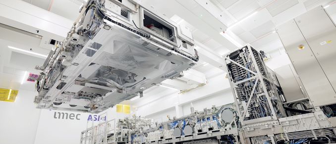
Imec and ASML have announced that the two companies have printed the first logic and DRAM patterns using ASML's experimental Twinscan EXE:5000 EUV lithography tool, the industry's first High-NA EUV scanner. The lithography system achieved resolution that is good enough for 1.4nm-class process technology with just one exposure, which confirms the capabilities of the system and that development of the High-NA ecosystem remains on-track for use in commercial chip production later this decade. "The results confirm the long-predicted resolution capability of High NA EUV lithography, targeting sub 20nm pitch metal layers in one single exposure," said Luc Van den hove, president and CEO of imec. "High NA EUV will therefore be highly instrumental to continue the dimensional scaling of logic and memory technologies, one of...
The Future of Silicon: An Exclusive Interview with Dr. Gary Patton, CTO of GlobalFoundries
In our recent trip to GlobalFoundries Fab 8, its leading edge facility, we managed to spend some time with the C-level executive that controls the future of this part...
39 by Ian Cutress on 2/24/2018
The AnandTech Podcast, Episode 45: GlobalFoundries and Fab 8
In early February, GlobalFoundries did something completely unexpected: for the second time in ten years, they invited a few select press and analysts to visit one of their fabrication...
14 by Ian Cutress on 2/20/2018
EUV Lithography Makes Good Progress, Still Not Ready for Prime Time
At the recent annual SPIE Advanced Lithography conference, Intel, TSMC and other leading semiconductor companies said that significant strides have been made in extreme ultraviolet lithography (EUVL) over the...
38 by Anton Shilov on 3/10/2016


