EUV
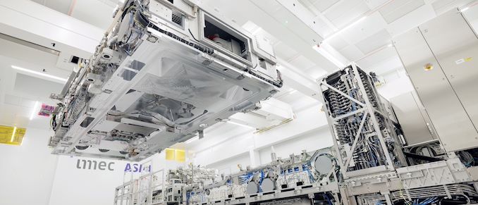
Imec and ASML have announced that the two companies have printed the first logic and DRAM patterns using ASML's experimental Twinscan EXE:5000 EUV lithography tool, the industry's first High-NA EUV scanner. The lithography system achieved resolution that is good enough for 1.4nm-class process technology with just one exposure, which confirms the capabilities of the system and that development of the High-NA ecosystem remains on-track for use in commercial chip production later this decade. "The results confirm the long-predicted resolution capability of High NA EUV lithography, targeting sub 20nm pitch metal layers in one single exposure," said Luc Van den hove, president and CEO of imec. "High NA EUV will therefore be highly instrumental to continue the dimensional scaling of logic and memory technologies, one of...

TSMC Starts to Build Fab 18: 5 nm, Volume Production in Early 2020
TSMC last week held a groundbreaking ceremony for its Fab 18 phase 1 production facility. The fab will produce chips using TSMC’s 5 nm process starting from early 2020...
27 by Anton Shilov on 1/31/2018
GlobalFoundries Details 7 nm Plans: Three Generations, 700 mm², HVM in 2018
Keeping an eye on the ever-evolving world of silicon lithography, GlobalFoundries has recently disclosed additional details about its 7 nm generation of process technologies. As announced last September, the...
76 by Anton Shilov on 6/23/2017
Samsung and TSMC Roadmaps: 8 and 6 nm Added, Looking at 22ULP and 12FFC
Samsung and TSMC have made several important announcements about the present and future of their semiconductor manufacturing technologies in March. Samsung revealed that it had shipped over 70 thousand...
89 by Anton Shilov on 5/5/2017
GlobalFoundries to Expand Capacities, Build a Fab in China
GlobalFoundries has announced plans to expand manufacturing capacities for its leading edge and mainstream production technologies in the U.S., Germany and Singapore. After the upgrades of the fabs are...
49 by Anton Shilov on 2/11/2017
Intel to Equip Fab 42 for 7 nm
Intel this week announced plans to bring its Fab 42 online to produce semiconductors using a 7 nm fabrication process. It will take three to four years, and the...
24 by Anton Shilov on 2/9/2017
GlobalFoundries Updates Roadmap: 7 nm in 2H 2018, EUV Sooner Than Later?
GlobalFoundries recently announced the first details about its next generation 7 nm manufacturing technology, which is being developed in-house, and revealed plans to start production of chips using the...
76 by Anton Shilov on 10/3/2016
Intel’s ‘Tick-Tock’ Seemingly Dead, Becomes ‘Process-Architecture-Optimization’
As reported at The Motley Fool, Intel’s latest 10-K / annual report filing would seem to suggest that the ‘Tick-Tock’ strategy of introducing a new lithographic process note in...
98 by Ian Cutress on 3/22/2016
EUV Lithography Makes Good Progress, Still Not Ready for Prime Time
At the recent annual SPIE Advanced Lithography conference, Intel, TSMC and other leading semiconductor companies said that significant strides have been made in extreme ultraviolet lithography (EUVL) over the...
38 by Anton Shilov on 3/10/2016


